
High voltage (120V), converting familiar fast (120V Shu us) power MOSFET Amplifier circuit
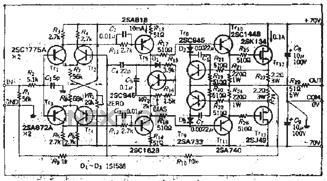
The described south circuit is a complex assembly of transistors designed for efficient signal processing and amplification. The NPN transistor (T1) acts as a dynamic garbage collector, filtering unwanted noise from the input signal. This is essential in maintaining signal integrity, particularly in environments with significant electromagnetic interference.
The PNP differential amplifier (T2, T3) operates as a double differential circuit, which enhances the circuit's ability to reject common-mode signals while amplifying the differential signal. This configuration is particularly beneficial in applications requiring high precision and stability, as it ensures that any noise common to both inputs is minimized.
The voltage amplification stage, utilizing photo transistors (T4, T5), is critical in determining the output amplitude. These transistors are designed to handle high bias voltages, which allows for better performance in terms of linearity and dynamic range. The absence of a phase compensation capacitor in the collector-base junction of T1 and T2 can lead to potential issues with conversion rates, particularly under varying load conditions.
The bias circuit serves a dual purpose: it stabilizes the output stage by eliminating unwanted voltage at the base and ensures that the circuit operates within a defined quiet area. This is crucial for maintaining performance, especially when the output stage is subjected to no-load conditions, where excessive current might otherwise flow.
Transistor T3 plays a vital role in protecting the output stage from short-circuit conditions by limiting the maximum drain current. This is a critical safety feature, ensuring that the circuit can withstand fault conditions without sustaining damage.
The voltage division described indicates a mechanism for controlling the activation of the transistors based on load conditions. When the voltage across the load reaches 0.5V, it triggers the transistor to turn on, thereby regulating the current flow and ensuring that the circuit operates within established domestic standards. This feature is essential for maintaining compliance with safety regulations and ensuring reliable operation in practical applications.
Overall, the south circuit is a sophisticated design that effectively combines various transistor configurations to achieve high-performance signal processing, amplification, and protection against faults, making it suitable for a wide range of electronic applications.The south circuit composed of four parts, the order of descent {NPN transistor whole dynamic garbage dog device (Tfl ", Tr song and PNP transistor differential amplifier Phi (TrS, Tt.4) double differential circuit, two balanced amplifier C output opposite phase), and the drive voltage amplification photo (Trs. Tri) port voltage amplifier stage is an important component determines the output amplitude and conversion Qu sneeze should be possible to work under a large bias Tong.
Because Tr ,, TT8 collector base valve without a vote plus phase compensation capacitor, it is possible to reduce the conversion rate of decline. Trr bias circuit is used to eliminate the base voltage of the output stage q quiet area with yR. You can not pay the entire signal current output stage (or no-load electric reservoirs); r_, Tr- is used to limit the maximum drain current of the output stage circuit, play load short-circuit protection.
Chu 1. , Set i. To reveal "the voltage across the 'I mouth lIi ,, x chu means D) dividing the voltage as Garnet had 0.5y, the transistor will be turned on by the suction 5fT'_l income TrIo base electric comb, so that electrical limit village gangrene in certain domestic norm.
Related Circuits
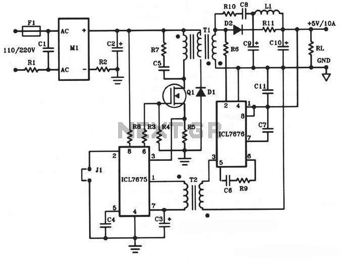
The following diagram illustrates a 50W offline switching power supply circuit design. This circuit is powered by a MOSFET, specifically the BUZ80A/IXTP4N8 for a 220V AC voltage input and the GE IRF823 for a 110V AC voltage input. The...
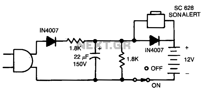
When the power is turned off, the alarm activates when switch S1 is closed. The 12-V battery remains charged when the circuit is connected and the switch is in the "on" position. The described circuit features an alarm system that...
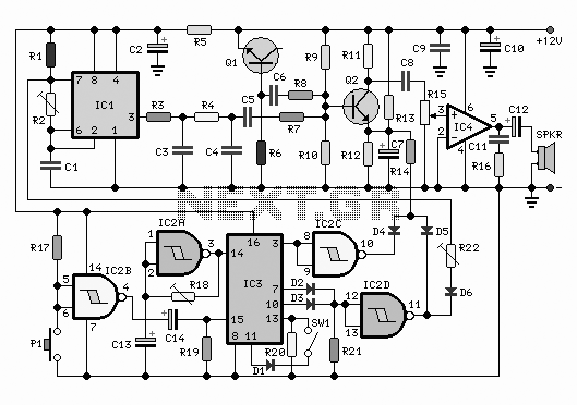
Cuckoo Sound Generator Circuit Schematic. This circuit generates a two-tone effect similar to the cuckoo song. It can be utilized for doorbells or other applications due to a built-in audio amplifier and loudspeaker. The Cuckoo Sound Generator Circuit is designed...
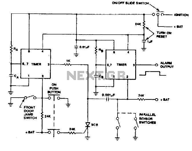
The 555 timer generates a reliable delay, enabling the driver to deactivate the alarm and eliminating the need for an external control switch that could be compromised. Additionally, the RCS prevents the activation of timer B unless it is...
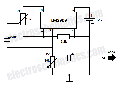
This circuit generates sine wave oscillations, but it can also be modified to produce triangle or square wave functions. The frequency is adjustable by varying the current. By disconnecting the 20k resistor (RIN) from the reference (REF) pin (pin...
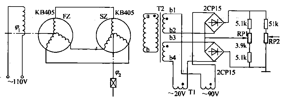
The transmitter (FZ) winding and receiver (SZ) correspond to the three-phase windings connected to a 110V AC voltage supply for transmission. The field winding, early start angle, and receiver output voltage at both ends of the stator windings reflect...
Warning: include(partials/cookie-banner.php): Failed to open stream: Permission denied in /var/www/html/nextgr/view-circuit.php on line 713
Warning: include(): Failed opening 'partials/cookie-banner.php' for inclusion (include_path='.:/usr/share/php') in /var/www/html/nextgr/view-circuit.php on line 713