
Hour time-delay sampling circuit

The described circuit employs a Programmable Unijunction Transistor (PUT) as the primary output switching device (Q2). The operation of this circuit hinges on the controlled charging and discharging of a capacitor, which is connected to the gate of the PUT. Initially, a high gate voltage is applied, allowing the capacitor to charge rapidly. This charging phase is crucial as it sets the stage for the subsequent operation of the circuit.
Once the capacitor reaches a certain voltage threshold, the gate voltage is periodically reduced. This reduction is essential as it influences the firing of the PUT (Q2). When Q1, which functions as an oscillator, fires, it creates a pulse that allows the timing resistor to regulate the current flowing through the circuit. The value of the timing resistor is critical; it must be chosen such that it limits the current to a level significantly lower than the peak current (IP). This design choice is important for protecting the circuit components from excessive current that could lead to failure.
The triggering mechanism relies on ensuring that the capacitor maintains a minimum charge during the oscillation period of Q1. This minimum charge is necessary to allow current to flow through the timing resistor, thus enabling the circuit to function as intended. The performance of the circuit is influenced not by the size of the capacitor but by its leakage characteristics and stability over time. High leakage can lead to insufficient charge retention, while instability can affect the timing and reliability of the circuit operation.
In summary, this circuit effectively manages the output current through careful control of the capacitor's charging and discharging cycles, utilizing the characteristics of the PUT and the timing resistor to achieve desired operational parameters.The circuit lowers the effective peak current of the output PUT, Q2. By allowing the capacitor to charge with high gate voltage and periodically lowering gate voltage, when Ql fires, the timing resistor can be a value which supplies a much lower current than IP. The triggering requirement here is that minimum charge to trigger flow through the timing resistor during the period of the Ql oscillator.
This is not capacitor size dependent, only capacitor leakage and stability dependent.
Related Circuits

The transistor characteristic curve tracer circuit depicted in Figure 555 illustrates the characteristics of a transistor. It utilizes two voltages: a step wave applied to the base (b) to generate different base currents (Ib), and a sawtooth waveform at...
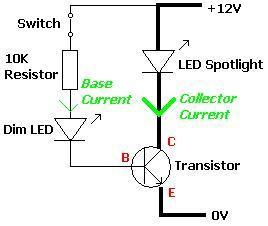
A transistor is an electronic component that allows a small current to control a significantly larger current. This characteristic is valuable in various renewable energy projects and other applications. A basic circuit diagram is provided, featuring a 12V LED...
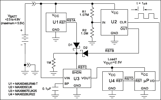
The micropower circuit automatically provides shutdown, power-up, and low-battery lockout functions without requiring software or operator control. The micropower circuit is designed to manage power efficiently in battery-operated devices, ensuring optimal functionality while conserving energy. The shutdown feature is activated...
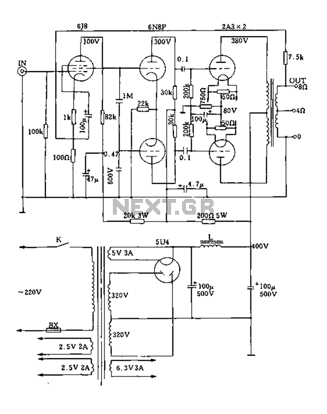
FIG. 2A3A is a low direct thermal resistance transistor with a resistance of only 800 ohms. The output transformer has a primary screen to load impedance of 3.5k ohms. The push-pull amplifier tube operates with a screen voltage ranging...
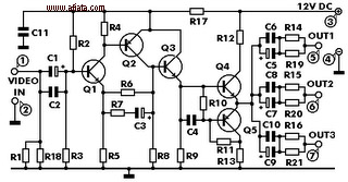
This electronic circuit is a video signal amplifier that provides a broad bandwidth amplifier with a capacity of 5 MHz. It is designed to take video signals from a VCR and amplify them adequately to drive up to three...

The precision Phase Locked Loop (PLL) in this circuit operates similarly to a basic PLL, but with several enhancements. The flip-flops in the detector are equipped with a gate G1 to clear them, allowing for a faster response. The...