
Hv440: High Voltage Ring Generator

The HV739 serves as a versatile component in high-voltage applications, particularly in the field of ultrasound technology. Its compact QFN package allows for integration into space-constrained designs while maintaining high performance. The ability to deliver significant current and voltage swings makes it suitable for driving various transducer types, ensuring effective signal generation and transmission. The integrated protection features enhance reliability, safeguarding the device during operation. The design's flexibility, including the rapid adjustment of supply voltages and the elimination of external coupling capacitors, contributes to streamlined development and testing processes. The high-speed level translators enable compatibility with a range of logic levels, making the HV739 adaptable to various control systems. Overall, the HV739 is a robust solution for applications requiring precise control of high-voltage pulsing, providing essential capabilities for both medical and industrial ultrasonic applications.The HV739 is a monolithic single channel, high-speed, high voltage, ultrasound transmitter pulser. This integrated, high performance circuit is in a single, 5x5mm, 32-lead QFN package. The HV739 CAN deliver up to a ±3. 0A source and sink current to a capacitive transducer. It is designed for the ultrasound material inspection NDT and medical ultra sound imaging applications. It CAN also be used as a high voltage driver for other piezoelectric or capacitive MEMS transducers, or for ATE systems and pulse signal generators as a signal source. HV739 ½ ½s circuitry consists of controller Logic circuits, Level Translators Gate driving Buffers and a high current and high voltage MOSFET output stage.
The output stages of each channel are designed to provide peak output currents over ±3. 0A for pulsing, with up to ±80 volt swings. Two‚oating 12VDC power supplies referenced to VPP and VNN supply the P- and N-type power FET Gate drivers. The upper limit frequency of the pulser waveform is 35MHz depending on the load capacitance. The HV739 CAN also be used as a damping circuit to generate fast return-to-zero waveforms by working with another HV739 as a pulsing circuit.
It also has built-in under-voltage and over-temperature protection functions. This demo board data sheet describes how to use the HV739DB1 to generate the basic high voltage pulse wave- form as an ultrasound transmitting pulser. The HV739 circuit uses the DC coupling method in all Level Translators There are no external coupling capacitors need- ed.
The VPP and VNN rail voltages CAN be changed rather quickly, compared to a high voltage capacitor gate-coupled driving pulser. This direct coupling topology of the Gate driv- ers not only saves two high voltage capacitors per channel, but also makes the PCB layout easier.
The input stage of the HV739 has high-speed level transla- tors that are able to operate with Logic signals of 1. 8 to 5. 0V volts and are optimized at 3. 3 to 5. 0V. In this demo board, the control Logic signals are connected to a high-speed rib- bon cable connector.
The control signal logic-high voltage should be the same as the VCC voltage of the demo board, and the logic-low should be reference to GND. The HV739DB1 output waveforms CAN be displayed using an oscilloscope directly by connecting the scope probe to the test point HVOUT and GND.
The soldering jumper CAN se- lect whether or not to connect the on-board equivalent-load, a 330pF, 200V capacitor, parallel with a 2. 5k ©, 1W resistor. A coaxial cable CAN be used to connect the user`s transducer to easily drive and evaluate the HV739 transmitter pulser.
🔗 External reference
Related Circuits
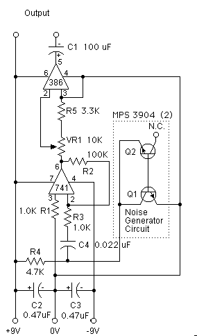
This circuit is effective for testing audio circuits using broadband noise. It employs three inexpensive C-MOS integrated circuits (ICs) that produce a series of output pulses with randomly varying widths. The audio noise generator is designed to drive earphones...
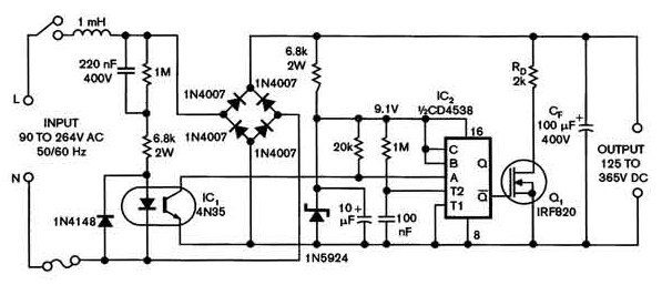
Universal power supply with a safe high-voltage capacitor power supply. Refer to that page to read the explanation about the related circuit diagram of the above power supply. The universal power supply circuit is designed to provide a stable output...
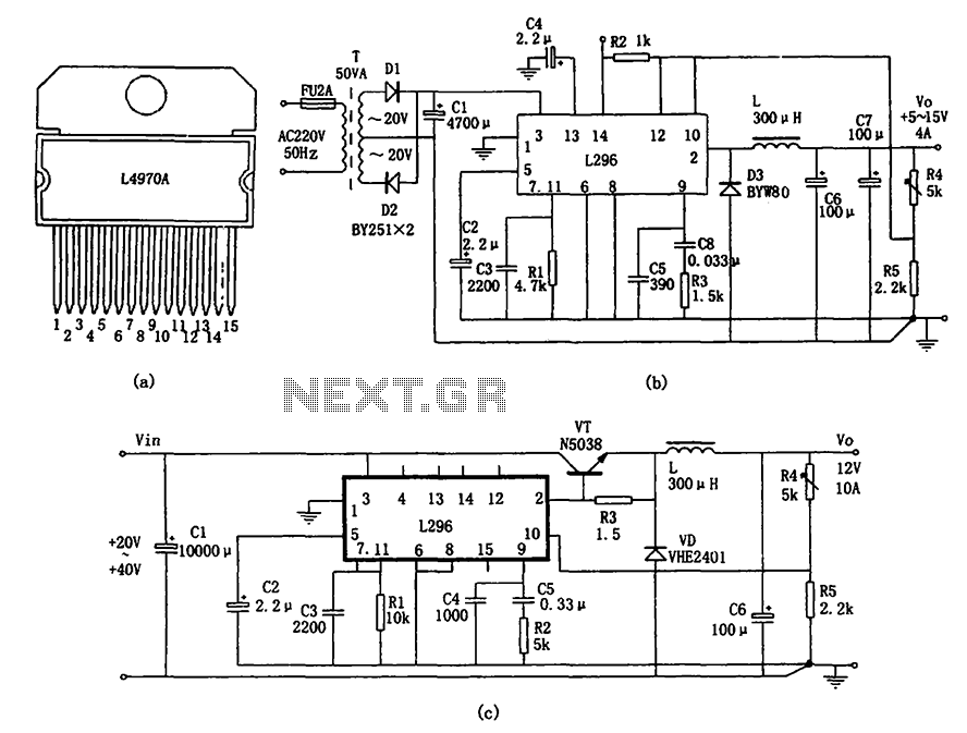
The L296 chip is a high-current switching power supply component designed to operate within a voltage range of 5 to 15V and provide an output current of up to 4A. This monolithic chip incorporates several features including enhanced protection...
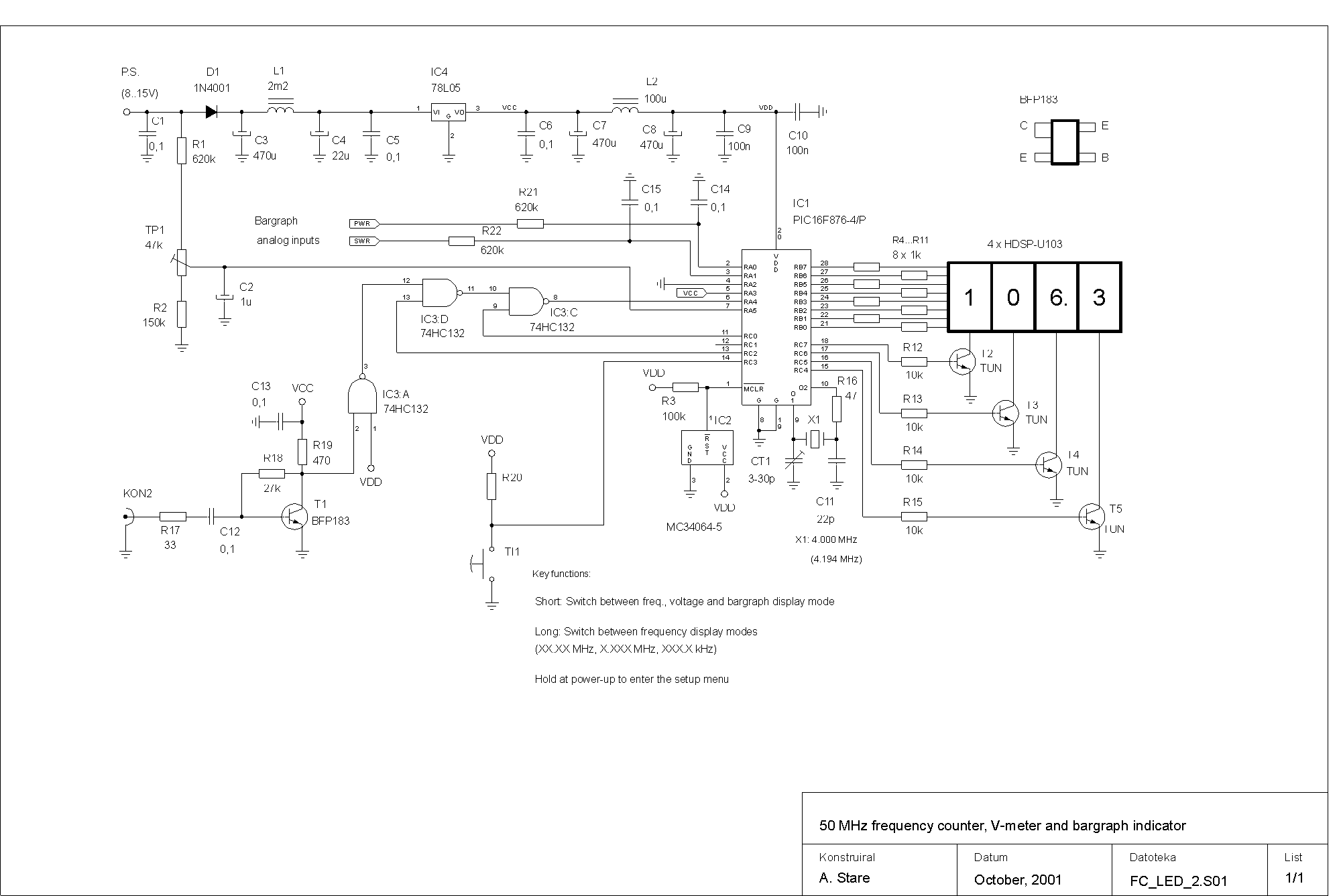
This device is a successor to the PIC16C71 4-digit LED frequency counter and voltmeter. It omits some hard-to-find components from the previous version that have been out of production for some time. The earlier PIC16C71 has been replaced with...
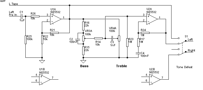
The preamp featured has optional tone and balance controls which may be omitted if desired. The input switching may be extended if needed to accommodate more signal sources. In this version, no RIAA (phono) input is provided. See the...
This preamplifier is a requirement resulting from many friends to provide a high-quality preamplifier, capable of driving high-quality power amplifiers with good sound. It is not, however, difficult to make; it combines simplicity and handiness. It does not allocate...