
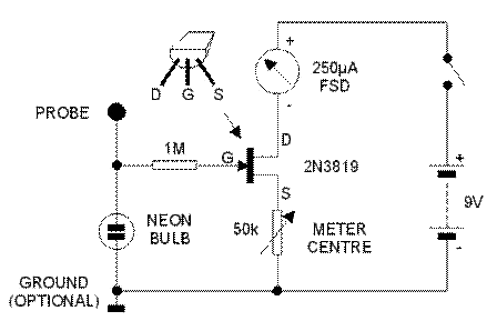
Inverter Schematics

The circuit design incorporates a biasing network consisting of resistors R1 and R2, which are strategically connected to the bases of transistors Q1 and Q2. This arrangement ensures that both transistors receive an initial forward bias, allowing them to enter conduction mode promptly when power is applied. The choice of resistors is critical; their values must be selected to provide sufficient biasing without overwhelming the base-emitter junctions of the transistors.
The use of integrated circuit timing circuitry is a significant enhancement to the inverter's operation. This circuitry can generate precise timing signals that control the switching of the transistors, leading to improved performance and reliability. High-quality core materials for the transformers are essential to minimize losses associated with magnetic hysteresis and eddy currents. The inclusion of JFETs may provide additional benefits, such as lower on-resistance and faster switching times, further optimizing the inverter's efficiency.
Transformer design is crucial for achieving the desired output frequency of 60 Hz. The physical dimensions of the transformer coils and cores must be sufficient to handle the required power levels while maintaining operational efficiency. If the circuit is intended for frequency inversion, the clock circuitry can be adjusted to operate at higher frequencies, such as 40 kHz. This adjustment allows for smaller transformer designs, which can lead to reduced core and winding losses. Additionally, operating at higher frequencies can help mitigate thermal issues associated with resistive losses, thereby enhancing the overall performance of the inverter system.
In summary, careful consideration of biasing, timing circuitry, transformer design, and component selection is vital for creating an efficient inverter circuit capable of meeting the specified operational requirements.A small bias on the bases of Q1 and Q2 via R1 and R2, assists in "starting" This gives each transistor`s base a small forward bias, so that both transistors tend to conduct when the circuit is first switched on [the base voltage on each transistor is zero when circuit is first switched on, so the small forward biasing thru R1 and R2 results in an above zero voltage at each base]. Use of IC timing [clock] circuitry, along with quality core materials for the transformers and possibly JFET`s wil increase the accuracy, and decrease the losses, making the Inverter more efficient. The transformers` coils and cores will need to be large, since the output Hz required is 60Hz. If this was part of a DC to DC converter, or if this was used for Frequency Inversion [input = low Hz, output = High Hz], then the clock circuitry can be set for a higher Hz.
like 40KHz [or what ever the output Hz will be]. Being up in that range will reduce the size of the transformers dramatically - which also increases efficiency by decreasing core losses, winding losses and losses from heat [winding resistance, core`s reluctance, etc. ]. 🔗 External reference
Related Circuits
The following circuit is an electronic approximation of the gold leaf electroscope, with the added capability of indicating both polarity and electric field magnitude. It is highly sensitive, capable of detecting a television or an electrostatically charged comb from...
It is relatively easy to find square wave inverter circuits online. However, to operate most loads such as fans and televisions, a sine wave inverter is required. Constructing a sine wave or near-sine wave inverter is more complex and...
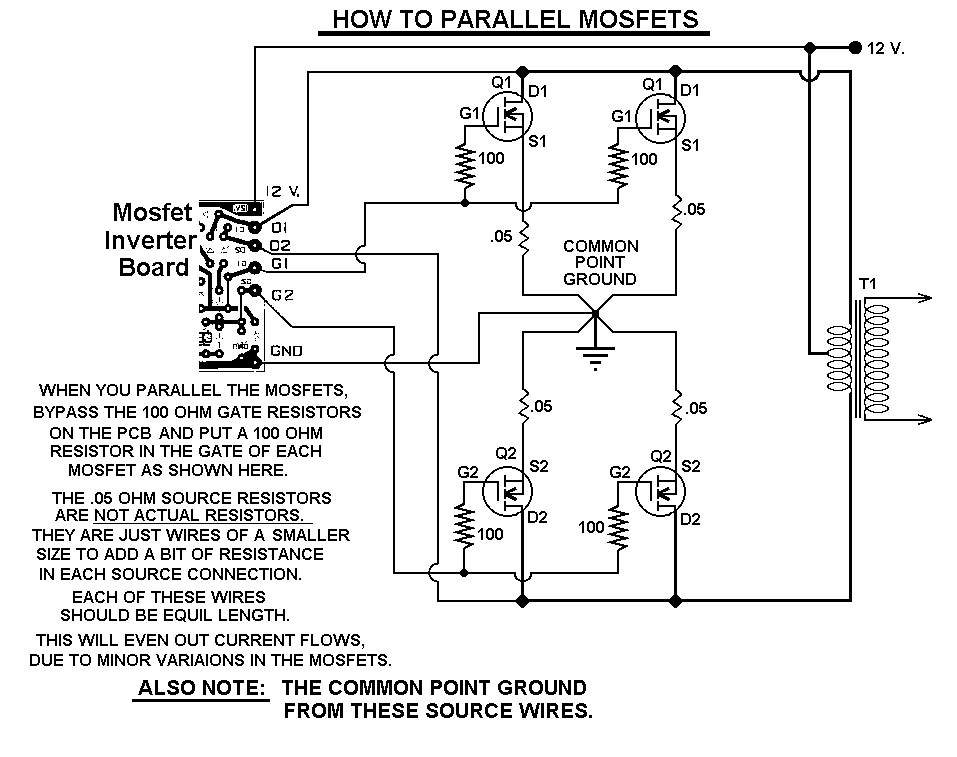
This 1000-watt power inverter circuit diagram utilizes the MOSFET RF50N06. To achieve higher power output, additional MOSFETs can be connected in parallel with the RF50N06. These MOSFETs are rated for 60 volts and 50 amps. It is essential to...
The design of a wireless data communication circuit is primarily intended for motor vehicles and fixed base station systems to facilitate close-range wireless data exchange. The circuit is based on the core chip nRF401 and its associated components. The...
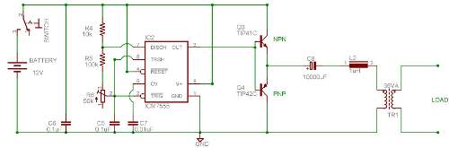
This circuit is a DC to AC inverter utilizing a 555 timer and a transformer with a specification of 9-0-9V/230V and a rating of 36VA. Key components include a 555 integrated circuit (IC), TIP42C, and TIP41C transistors. The described circuit...
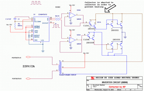
This circuit converts 12V DC into 220V AC. It utilizes a 4047 integrated circuit to generate a 50Hz square wave, which is then used to amplify the current and subsequently increase the voltage using a step-up transformer. The circuit...