
Low Noise And Drift Composite Amp Circuit
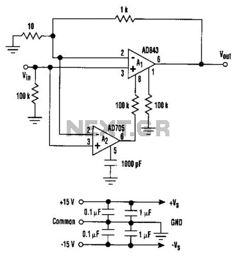
The described circuit configuration represents a sophisticated approach to achieving enhanced performance in operational amplifiers by utilizing a composite design that leverages both FET and bipolar technologies. The high-speed FET input operational amplifier (A1) is specifically designed to provide rapid response times and excellent bandwidth, making it suitable for applications requiring quick signal processing. The closed-loop gain of 100 ensures that the output signal is amplified significantly while maintaining signal integrity.
The integration of the SuperBeta bipolar input operational amplifier (A2) introduces a mechanism for improving the input offset voltage and drift characteristics of the system. By monitoring the input voltage at A1 and dynamically adjusting the current injected into the null pins, A2 effectively compensates for any discrepancies that may arise due to temperature variations or component tolerances. This feedback loop is crucial in maintaining the desired performance levels, particularly in precision applications where accuracy is paramount.
The choice of a source impedance of 100 kΩ is notable, as it balances the trade-off between noise performance and input impedance. A higher source impedance can lead to increased noise, but in this configuration, the low noise characteristics of A2 help mitigate these effects, thereby preserving the overall signal quality.
This composite amplifier circuit is ideal for applications requiring high precision, such as instrumentation and sensor interfacing, where maintaining low offset and drift is essential for accurate measurements. The synergy between the FET and bipolar technologies in this design exemplifies an advanced engineering solution tailored for high-performance electronic systems. This circuit offers the best of both worlds. It can be combined with a low input offset voltage and drift without degrading the overall system`s dynamic performance. Compared to a standalone FET input operational amplifier, the composite amplifier circuit exhibits a 20-fold improvement in voltage offset and drift.
In this circuit arrangement, A1 is a highspeed FET input op amp with a closed-loop gain of 100 (the source impedance was arbitrarily chosen to be 100 kfl). A2 is a SuperBeta bipolar input op amp. It has good dc characteristics, biFET-level input bias current, and low noise. A2 monitors the voltage at the input of A1 and injects current to Al`s null pins. This forces A1 to have the input properties of a bipolar amplifier while maintaining its bandwidth and low-input-bias-current noise. 🔗 External reference
Related Circuits
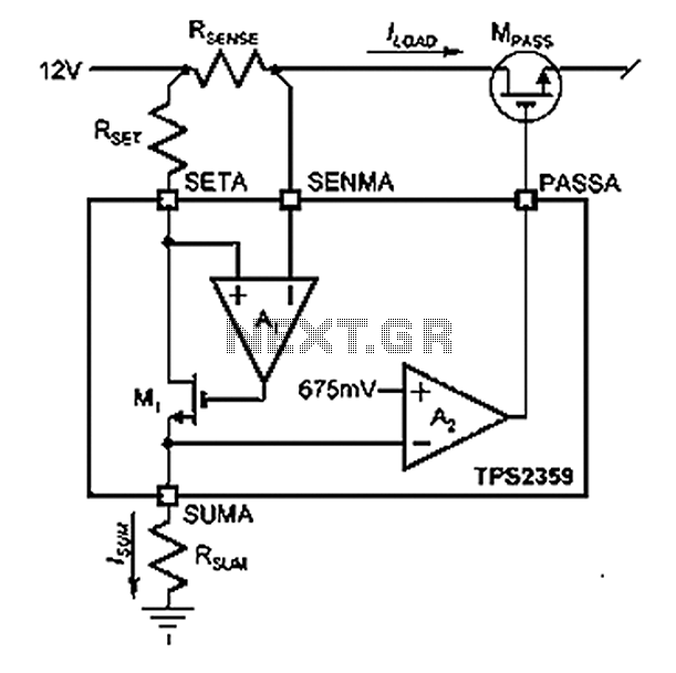
Amplifier A1 utilizes the voltage across the sense resistor sensors to monitor the load current ILOAD. The power management channel employs a similar circuit, with the distinction of integrating resistors RSENSE and RSET. Amplifier A1 is configured to measure the...

The timer is activated by the zero-crossing voltage pulse. The time constant is defined by the combination of C5 and the resistors R14 and R15, which determines the conduction angle. The transistors T2 and T3 prevent the power switch...
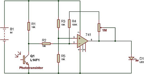
This versatile 741 operational amplifier module can be utilized to create a dark detector using a light-dependent resistor (LDR), a phototransistor, and a photodiode. The amplifier is configured in inverting mode, where it compares the voltage change at pin...
Current leakage protection is the most commonly used and effective leakage protection device. Current leakage protectors can be divided into electromagnetic and electronic types. The zero-sequence current transformer serves as the detection element, while electromagnetic leakage protection uses a...
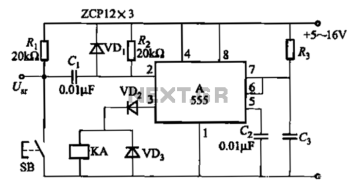
The 555 integrated circuit is utilized in a delay circuit configuration, functioning as a one-shot timer. The delay time can be adjusted using resistor R3 and capacitor C3. Typical values for R3 range from 1 kΩ to 10 MΩ,...
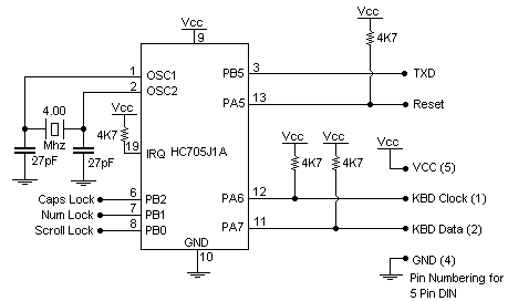
This document details the AT Keyboard Interface and AT Keyboard Protocols. It includes an example of a Keyboard to ASCII decoder utilizing a 68HC705J1A microcontroller. The AT Keyboard Interface is a standard communication protocol used primarily in personal computers to...
Warning: include(partials/cookie-banner.php): Failed to open stream: Permission denied in /var/www/html/nextgr/view-circuit.php on line 713
Warning: include(): Failed opening 'partials/cookie-banner.php' for inclusion (include_path='.:/usr/share/php') in /var/www/html/nextgr/view-circuit.php on line 713