
Low power timer switch

The timing circuit described operates effectively by leveraging the characteristics of the 555 timer in conjunction with discrete electronic components. The use of F1 and F2 as electronic switches allows for a significant reduction in quiescent current, enhancing the efficiency of the circuit during idle states. The operation begins with the application of power, at which point capacitor C2 remains uncharged, preventing immediate changes in voltage. This leads to F2 achieving a high state, which in turn locks F1 in a low state, effectively disabling the output of VT1 and minimizing current draw.
When the timer switch AN is engaged, it introduces a negative pulse to the input of F1. This pulse is critical as it triggers F1 to switch to a high output state, thereby activating VT1. Consequently, the 555 timer receives its supply voltage, enabling its operational capabilities. The application of the negative pulse to pin 2 of the 555 timer is equally important, as it sets the timer into motion, commencing the timing cycle.
The duration of the timing cycle, represented by td, is directly influenced by the components R4 and C3. The formula td = 1.1 * R4 * C3 indicates that the timing period can be extended or reduced by varying either the resistance of R4 or the capacitance of C3. This flexibility allows for customization of the timing circuit to suit various applications, making it a versatile solution for timing-related tasks in electronic designs. As shown, the timing circuit due to the installation of the electronic switch by the F1, F2 and VT1 composed of quiescent current can be reduced to 555 l ~ 2 A. When the power is first turned on, since the voltage on C2 can not jump, so F2 gate goes high, F1 to lock in a low output potential, VT1 off, so that the quiescent current of the entire circuit is small. When you press the timer switch AN, F1 input of a negative pulse appears, F1 output goes high, VT conduction, only the supply voltage 555.
At the same time, due to the negative pulse is applied to 555 feet 2, 555 set, K Pull, the timer starts. Timing td 1.1R4C3. Timing can be changed by adjusting the length of the time constant R4C3 of.
Related Circuits
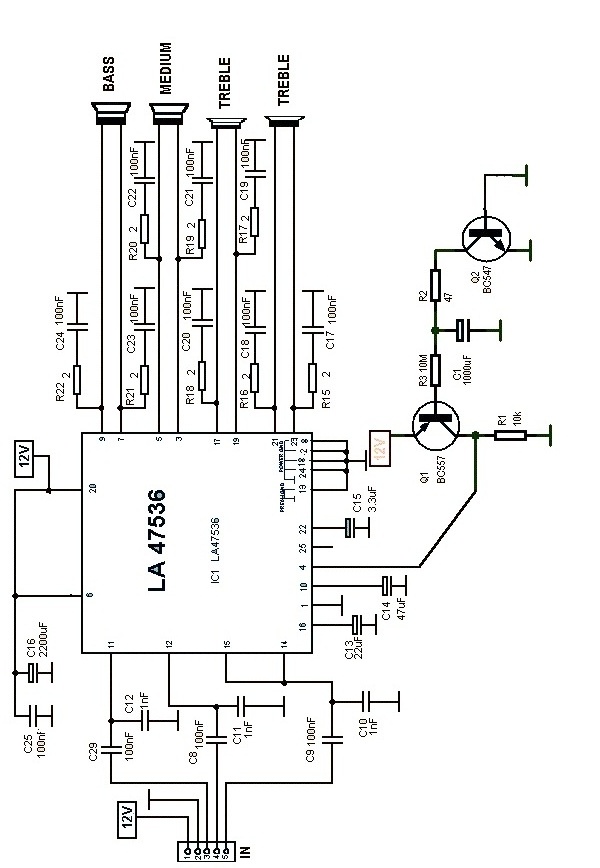
This car audio amplifier circuit is based on the LA47536 audio amplifier integrated circuit designed by Sanyo. This audio amplifier circuit is specifically designed for car audio power amplifiers. The LA47536 car audio amplifier IC features four output channels...
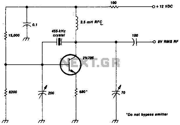
This crystal-oscillator circuit utilizes a 455-kHz crystal. It is a straightforward project. The crystal oscillator circuit based on a 455-kHz crystal operates by utilizing the piezoelectric properties of the crystal to generate a stable frequency. The circuit typically consists of...
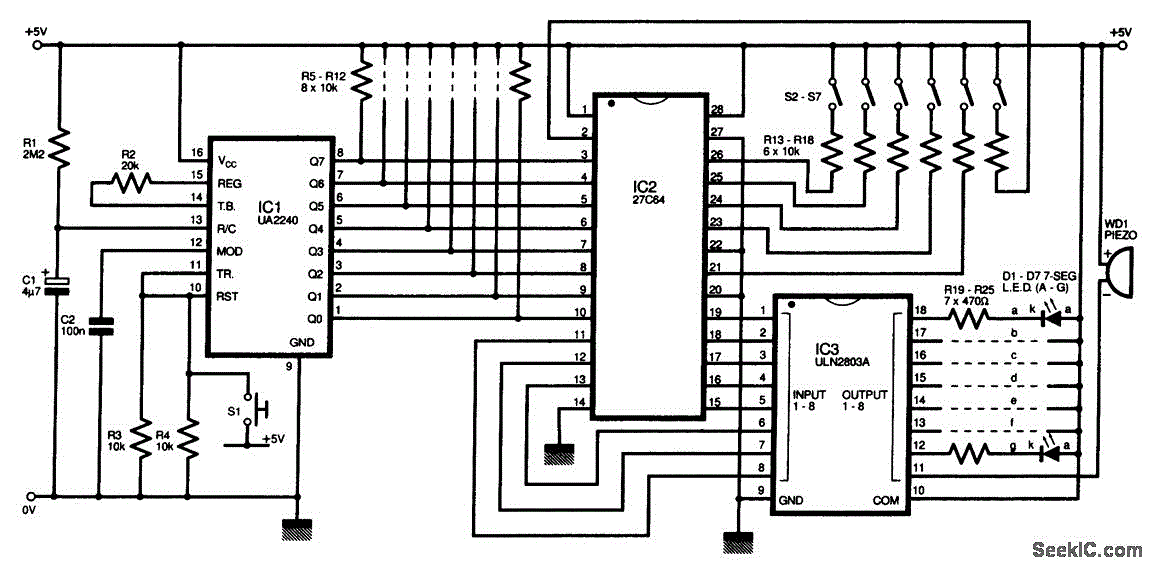
The circuit diagram of this programmable sequencer can be utilized for various timing applications. An audible tone is generated before the start of each interval, while a seven-segment LED display indicates the current interval number. A buzzer sounds again...
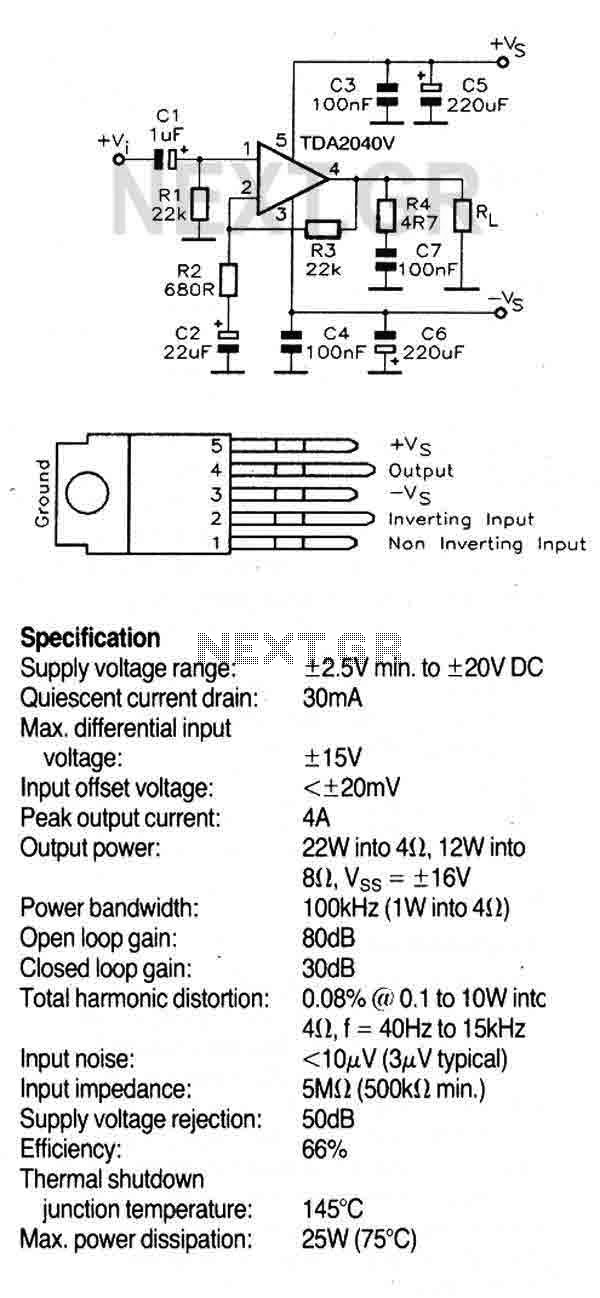
This circuit utilizes the TDA2040V, a monolithic power amplifier integrated circuit designed for high-quality, class AB audio amplification. It typically delivers 22W of output power into a 4-ohm load with a distortion level of 0.5%, powered by a 32V...
Stationary - MOPLL & Silicon Tuner TUA6020 2 Band TV Tuner Mixer-Oscillator-PLL with balanced IF-Amplifier. The TUA6020 device integrates a digitally programmable Phase Locked Loop (PLL) with a mixer-oscillator block that includes two balanced mixers and oscillators suitable for...
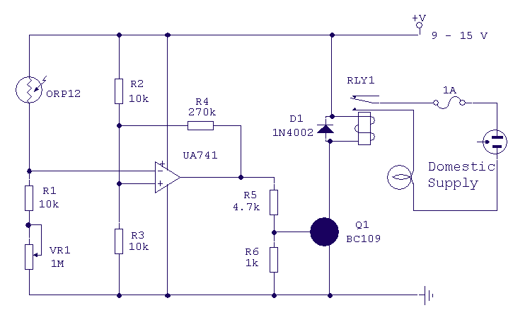
This circuit will activate a relay when light falls to a preset level. Light level can be adjusted with VR1 and the relay contacts may be used to operate an external light or buzzer. More: The light sensor used...