
low power universal demultiplexer decoder

The universal decoder circuit is designed to provide versatile functionality for various digital applications by allowing the selection between a dual or single decoding mode. In the dual 1-of-4 mode, each decoder section operates independently, providing four outputs based on the binary inputs A0 and A1. The active-LOW enable inputs ensure that the outputs are only activated when the corresponding enable signal is LOW, allowing for controlled operation in multi-device environments.
In the single 1-of-8 mode, the decoder combines the two sections into one, allowing for eight outputs based on three binary inputs (A0, A1, A2). The configuration of the inputs allows for a straightforward design where the outputs can be easily interfaced with other digital components. The inclusion of pull-down resistors on all inputs minimizes the risk of floating states, ensuring stable operation.
The circuit's adaptability makes it suitable for applications in data routing, multiplexing, and digital signal processing, where different modes of operation are required based on the system's needs. The design supports efficient use of space and resources, making it an ideal choice for integrated circuit implementations.This is a circuit for universal decoder that has functions as either a dual 1-of-4 decoder or as a single 1-of-8 decoder, depending on the signal applied to the Mode Control (M) input. Here`s the figure of the test circuit; In the dual mode, each half has a pair of active-LOW Enable (E) inputs.
Pin assignments for the E inputs are such that in the 1-of-8 mode they can easily be tied together in pairs to provide two active-LOW enables (E1a to E1b, E2a to E2b). Signals applied to auxiliary inputs Ha, Hb and Hc determine whether the outputs are active HIGH or active LOW.
In the dual 1-of-4 mode the Address inputs are A0a, A1a and A0b, A1b with A2a unused (i. e. , left open, tied to VEE or with LOW signal applied). In the 1-of-8 mode, the Address inputs are A0a, A1a, A2a with A0b and A1b LOW or open. All inputs have 50 kX pull down resistors. [Circuit diagram source: National Semiconductor Application Notes] 🔗 External reference
Related Circuits
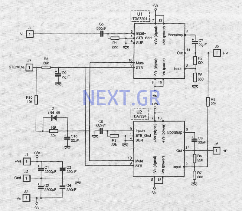
The TDA 7294 from T-MICROELECTRONICS is a monolithic integrated circuit housed in a "Multiwatt 15" package, primarily designed for use in Class AB amplifiers for high-fidelity applications, including stereo systems, active speakers, and television receivers. Its large feed area...
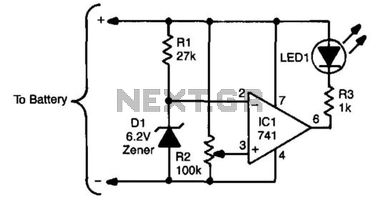
The sensing circuit consists of a 741 op-amp configured as a voltage comparator, utilizing a zener diode as a voltage reference. The op-amp is positioned as a bridge between two resistor ladders; one includes the zener reference, while the...
This circuit detects low-voltage supply conditions, down to 0.6 V. Diode D1 sets the trip point of the circuit. The circuit is useful for protecting memory circuits from accidental writes during low-voltage power supply conditions, which can cause other...
The IEEE 802.3af standard defines the interaction between power-sourcing equipment and powered devices within a power-over-Ethernet system. The IEEE 802.3af standard, also known as Power over Ethernet (PoE), specifies the mechanisms by which electrical power is transmitted alongside data over...
This circuit was designed to allow a laptop computer to be powered from a solar power setup. The computer requires 12V at 3.3A. The circuit is a linear regulator. The circuit functions as a power supply system that converts the...
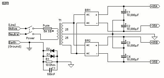
For the 60W amplifier, a nominal (full load) supply of +/- 35V is required, so a 25-0-25 secondary is ideal - however, see Updates, below. The circuit for the supply is shown below, and uses separate rectifiers, capacitors and...