
MAX12557 Schematic and Layout Suggestions

High-speed data converters are critical components in modern electronic systems, requiring careful consideration of their integration into printed circuit boards (PCBs). Effective PCB layout is essential to ensure optimal performance and reliability of these devices. The application note outlines several key guidelines that should be followed during the design phase.
Firstly, the layout of the PCB should minimize the length of the signal paths to reduce inductance and capacitance effects that can degrade signal integrity. This involves placing components such as data converters, amplifiers, and associated passive components in close proximity to each other. Additionally, using differential signaling can help mitigate noise and improve signal quality.
Bypassing and decoupling capacitors play a crucial role in maintaining stable power supply voltages and minimizing voltage fluctuations during high-speed operation. It is recommended to place these capacitors as close as possible to the power pins of the data converters. The use of low-ESR (Equivalent Series Resistance) capacitors is advised to ensure effective high-frequency performance.
Furthermore, ground planes should be employed to provide a low-impedance return path for signals, which helps to reduce electromagnetic interference (EMI) and enhances the overall performance of the circuit. Careful attention should also be paid to the routing of high-speed signals to avoid crosstalk and other forms of interference.
In summary, the application note serves as a comprehensive guide for engineers and designers working with high-speed data converters, emphasizing the importance of strategic PCB layout, effective bypassing, and decoupling techniques to optimize device performance. Following these guidelines will contribute to the reliability and efficiency of electronic systems utilizing high-speed data conversion technology.This application note provides valuable PC board layout, bypassing and decoupling guidelines for customers who are implementing high-speed data converters in their designs.. 🔗 External reference
Related Circuits

Utilizing sunlight as a power source can help reduce electricity costs. Below is a description of a simple power plant that can be created to charge a motorcycle battery or power emergency lights. Solar panels capture sunlight and convert...

This circuit schematic produces a beep and/or illuminates an LED when someone touches the door handle from outside. The alarm will continue to sound until the circuit is switched off. The circuit operates on the principle of capacitive sensing, where...
The ASIC design focuses on a highly integrated, low-power solution with a short development cycle to complete an FPGA design aimed at achieving a robust background system, which holds significant practical relevance and broad market potential. The project utilizes...

A low-cost solution for charging both NiCd and NiMH batteries is presented. The circuit diagram illustrates a universal charger designed for these battery types. The circuit for the low-cost universal charger for NiCd and NiMH batteries typically incorporates several key...
Specializing in unique and hard-to-find CB radio books, plans, kits, modifications, repairs, technical information, and high-performance CB accessories since 1976. The focus on CB (Citizens Band) radio equipment encompasses a wide array of products and services tailored to enthusiasts and...
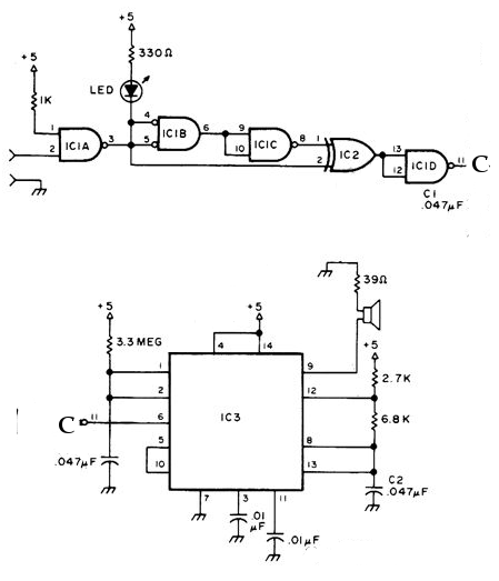
The NE556 timer can function as an indicator for the static state of a digital logic audible terminal. An audible logic probe is beneficial for visually inspecting a component while simultaneously checking the logic state at another point far...