
MAX8632 PCB Layout Optimization
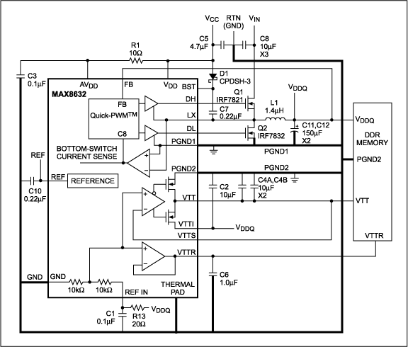
The MAX8632 Integrated DDR Power Supply is designed to efficiently deliver power to DDR memory modules, ensuring stable operation under varying load conditions. The synchronous buck controller is pivotal in achieving high efficiency during the conversion of input voltage to the VDDQ rail, which typically operates at voltages required by DDR memory, such as 1.5V or lower. This efficiency is crucial for minimizing thermal dissipation and enhancing overall system reliability.
The 3 Amp LDO regulator included in the MAX8632 architecture provides additional functionality by generating the VTT bus termination voltage, which is essential for maintaining signal integrity in DDR systems. This regulator can both source and sink current, allowing it to adapt to the dynamic load requirements of the DDR memory. The ability to sink current is particularly important during read operations, where the memory may draw current from the termination voltage.
Furthermore, the 15mA VTTR reference buffer serves as a stable reference voltage for the termination bus, ensuring that the VTT voltage remains consistent and within specified limits. This stability is critical for minimizing voltage fluctuations that could lead to data corruption or memory instability.
In terms of PCB layout, careful attention must be paid to the placement of components to minimize noise and optimize performance. The power traces should be designed to handle the load currents while minimizing inductance, and decoupling capacitors should be placed close to the power pins of the MAX8632 to ensure effective filtering of high-frequency noise. Ground planes should be utilized to provide a low-resistance return path, enhancing the overall performance of the power supply circuit.
This comprehensive design approach ensures that the MAX8632 Integrated DDR Power Supply operates effectively in a wide range of applications, delivering reliable power to DDR memory systems while adhering to strict performance and efficiency standards.This paper outlines a clear printed circuit board layout for implementation of the MAX8632 Integrated DDR Power Supply. This chip functions as an integrated DDR Power-Supply Solution that utilizes a synchronous-buck controller to generate VDDQ main rail, a 3 Amp high speed LDO (Low Drop Out) regulator that can source and sink current to generate VTT bus termination and a 15mA VTTR reference buffer..
🔗 External reference
Related Circuits
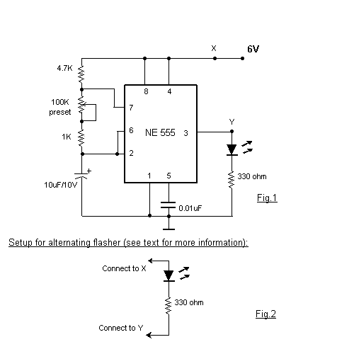
This circuit is a basic design for flashing one or more LEDs, as well as for alternately flashing multiple LEDs. It employs a 555 timer configured as an astable multivibrator, allowing for variable frequency operation. When the preset is...
That's right, Electric is open source! You can download Electric from the web for free. There is no better way to get to know a CAD system than to use it for a while. Now you can use it...
This circuit was designed to assist in the installation of TV antennas. The signal is monitored using a small portable TV set, and this circuit monitors the output of the TV's FM detector IC via a shielded lead. To...
The source code features a FAT12 filesystem that can be utilized to create custom flash drives for various projects. This source code is based on the Microchip Applications libraries for the Device Mass Storage SD Card data logger using...
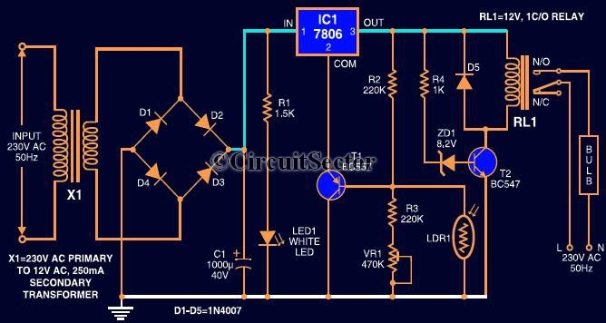
This circuit automates the control of street or porch lights. The automatic lamp controller circuit utilizes a 7806 voltage regulator IC, which can be employed to automate street lights, tube lights, or any other home electrical lighting systems. The...

This circuit is a low-cost, one-touch doorbell using a Bel 188 transistor. It is likely one of the most economical bell circuits that can be constructed. The core component of this circuit is the output transformer from a push-pull...
Warning: include(partials/cookie-banner.php): Failed to open stream: Permission denied in /var/www/html/nextgr/view-circuit.php on line 713
Warning: include(): Failed opening 'partials/cookie-banner.php' for inclusion (include_path='.:/usr/share/php') in /var/www/html/nextgr/view-circuit.php on line 713