
Shift register
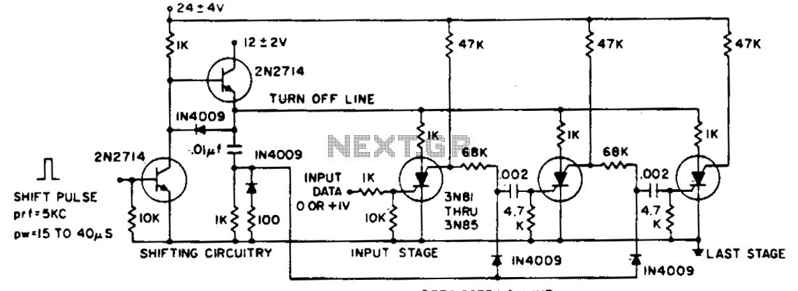
The described circuit operates on a shift pulse mechanism, which is characterized by an amplitude of less than 15 volts. This pulse serves as a control signal for a multi-stage system, where each stage can be either active or inactive. When a stage is inactive (off), the shift pulse is effectively blocked and does not propagate to the subsequent stage, ensuring that only active stages can influence the operation of the following components.
In an active stage, the presence of the shift pulse allows for conduction through a diode, which serves as a pathway for the pulse to trigger the next stage in the chain. This mechanism is crucial for cascading operations where the output of one stage directly influences the input of the next. The timing of the shift pulse is critical, as it determines the sequence of operation among the stages.
Before the shift pulse is applied, there is a deliberate interruption of the anode supply, which serves to deactivate all stages. This interruption ensures that the system is in a known state before the shift pulse is introduced, thus preventing any unintended triggering of stages.
The charge stored in the capacitors plays a pivotal role in determining which stages will be re-triggered upon the application of the shift pulse. The voltage across these capacitors influences the threshold at which the stages can be activated, allowing for selective triggering based on the previous state of the system. This design is particularly useful in applications requiring precise control over multiple stages, such as in digital signal processing or sequential logic circuits.The shift pulse amplitude is less than 15 volts. If a stage is off, the shift pulse will not be coupled to the next stage. If it is on, the diode will conduct triggering the next stage. Just prior to the shift pulse the anode supply is interrupted to turn off all stages. The stored capacitor charge determines which stages will be re triggered. 🔗 External reference
Related Circuits
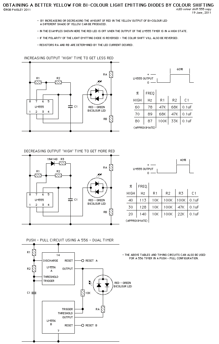
These circuits provide a means of altering the YELLOW output of RED / GREEN type two colour light emitting diodes. These circuits use the LM555 timer chip. The circuit described utilizes the LM555 timer integrated circuit (IC) to modulate the...
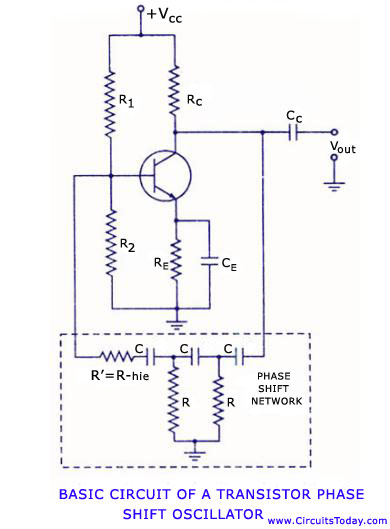
Transistor RC phase shift oscillator. RC phase shift oscillator using operational amplifier. RC phase shift network. Theory and working principle. Circuit diagram. The transistor RC phase shift oscillator is a type of electronic oscillator that generates sine wave signals. This...

Circuit characteristics: A simple phase shift range of 180 degrees, with a practical range of 170 degrees. The circuit is influenced by temperature and is suitable for small power applications in less demanding situations. The circuit operates by utilizing a...

The circuit features a shift register chip (74HC595N), which is not available on CircuitLab. There may be a specific representation for a shift register in schematic diagrams. Although assistance with CircuitLab is not provided, schematic illustrations can be referenced...
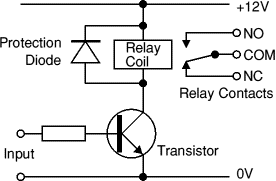
Replacing the resistor/transistor with an n-channel power MOSFET and substituting the relay/protection diode with a light bulb results in a simplified circuit that mirrors the original design, provided one end of the light bulb is connected to +12V. If...
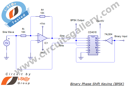
In a binary phase shift keying (BPSK) modulation scheme, the phase of a carrier signal is altered according to digital pulse signals. The BPSK modulator functions as a phase modulator, where the transmitted signal is a sinusoid with a...