
Micromouse Sensors
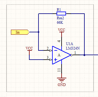
The circuit design begins with the conversion of current to voltage, adhering to the equation Vout = -Iin * R. The resistor value is chosen based on the expected current, with a selection of 66 kΩ to accommodate potential digital potentiometers. The positive terminal of the operational amplifier (op-amp) is connected to Vcc, creating a virtual ground at Vcc and allowing the output voltage to range from 5V to 0V. A difference amplifier is then employed to subtract the input voltage from Vcc, resulting in a signal range from 0V to 5V. An optional gain can be added at this stage, with the output voltage calculated using Vout = (V2 - V1) * (Rb / Ra), where Ra = R2 = R4, Rb = R3 = R5, V1 is the input voltage, and V2 is Vcc.
The design incorporates a second-order high-pass filter with a cutoff frequency set at 530 Hz. Although this is lower than the intended 10 kHz modulation frequency, it stems from an initial design based on 1 kHz modulation. Adjusting resistor values to 1 kΩ would shift the cutoff to approximately 1.6 kHz, which may be more suitable. The primary noise to be mitigated includes DC and 50 Hz mains noise, making the current values adequate for the design's purpose.
A peak detect and hold circuit is constructed using two op-amps. The voltage is stored in capacitor C3, which is compared with the current input at the left op-amp. If the input voltage exceeds the stored voltage, the op-amp operates as a voltage follower, increasing the output. The left op-amp functions as a buffer, with resistor R8 supplying current to prevent C3 from discharging. A MOSFET is included to enable the discharge of the capacitor after the analog-to-digital (A/D) conversion is completed.
Simulation of this circuit using LTSpice was conducted with input currents of 40 µA and 50 µA, alongside a 5 µA noise signal at 50 Hz. The simulation results illustrate various signal stages: the dark blue signal represents the output after the difference amplifier, the green signal follows the second-order high-pass filter, the red signal indicates the final output from the peak detect and hold circuit, the light blue signal denotes the peak detector's reset signal, and the pink signal represents the 50 Hz noise. The results demonstrate the noise's impact on the dark blue signal, its removal at the peak of the green signal, and the retention of the peak value as intended.Ok, its been a while since I did much more than think about my micromouse, but over the last week or so I actually did some work` on the sensor design First off this is all theoretical, I need some bits an pieces before I can test this outside of simulation. Hopefully in the next week or so I will order the bits I need. Commonly optical sensors are used which act upon the basic premise that the diameter of a cone of light will get bigger as it travels, hence the intensity of light over a specific sensing area will vary with the distance the light has traveled. There are also other factors such as scattering and the reflectivity of the surface etc. etc. but there is a correlation, that`s the main point. I am concerned with detecting the intensity of the light reflected, and removing any noise. My current design assumes that I have a source transmitting IR light at 10KHz and a receiver which converts received light to a current (such as a phototransistor).
First I convert this current to a usable voltage, then filter it to remove the noise and then I use a peak detect and hold circuit to get the sensor reading. This stage is quite simple, it takes the current and produces a voltage following the rule Vout = -Iin * R.
The value of the resistor should be selected based on the current expected. I chose 66K as I am considering having some digital potentiometers in there, and that`s there value. Notice that the positive terminal of the opamp is connected to Vcc, this creates a virtual ground at Vcc allowing it to go from 5V down the 0V. Because of this the voltage is now upside down` so the next bit of the circuit fixes this. This is a difference amplifier which takes Vcc and subtracts out voltage from it, meaning the signal goes from 0V to 5V.
Although not shown here you could also add in a gain here if required. The formula is Vout = (V2 V1) * (Rb / Ra) where Ra = R2 = R4, Rb = R3 = R5 and V1 is our voltage and V2 is shown here as Vcc. This is a standard second order high pass filter set to 530Hz cut-off. Considering I am aiming for 10kHz modulation this is quite low, but its due to the fact that I started with 1kHz modulation.
Changing the resistor values to 1K will change the cut-off to 1. 6kHz which is probably a bit safer. The main noise I wanted to remove was DC and mains (50Hz), so the current values will suffice for now. This is the one part of the circuit which is not required, but does help and remove any precise timing issues with converting the final voltage to a digital number.
The two opamps create a peak detect and hold circuit. The voltage is stored` in C3, the voltage here is compared with the current input on the left opamp, if it is higher the opamp acts as a voltage follower and increased the output. The opamp on the left is a buffer, I think R8 provides some current to keep C3 from discharging, its the only part of the circuit I don`t full understand yet.
I added a mosfet to enable the capacitor to be discharged after the A/D has completed. Using LTSpice I simulated this circuit with 40uA and 50uA inputs, with a 5uA @ 50Hz noise` sign wave. Left is a small segment of the result. The dark blue signal is the output after the Difference Amplifier, the green signal is after the second order high pass filter, the red is the final output from the peak detect and hold, the light blue is the peak detectors reset signal and the pink is the 50Hz noise (scale in A and on other axis).
You can see the noise affecting the dark blue signal, and being removed at the peak of the green signal, and the result being held at this peak as required. 🔗 External reference
Related Circuits

The LMP91200 is a configurable sensor analog front-end (AFE) designed for managing low-power analytical sensing applications, specifically for 2-electrode sensors. This device offers all the necessary functionality to detect changes based on a delta voltage from the sensor. It...
Strain-gauge sensors convert strain into an electrical signal for applications in pressure sensors, weight measurements, force and torque measurements, and materials analysis. A strain gauge functions as a resistor, with its resistance value changing in response to strain. Strain-gauge sensors...
This article explains how platinum resistance temperature detectors (PRTDs) can perform measurements over wide temperature ranges of -200 °C to +850 °C, with absolute accuracy and repeatability better than ±0.3 °C, when used with modern processors capable of resolving...
Interfacing the LM335A temperature sensor with A/D converters involves measuring temperature using the LM35 and LM335A sensors alongside the 9S12 HCS12 microcontroller. This process includes analyzing both calibrated and uncalibrated temperature errors of integrated circuit temperature sensors. The LM335A is...
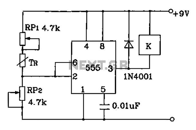
Adjust RP1 and RP2 to set the preset temperature control point. The 555 circuit is configured as a Schmitt inverter circuit that automatically controls a relay device. This forms part of the T-121 temperature control circuit, which includes a...
An effort is being made to enhance the responsiveness of an electronic keyboard due to dissatisfaction with the current sensitivity to keystrokes. The initial step in this process involves measuring the speed of the fastest keystroke. To improve the responsiveness...