
Microphone AGC amplifier
Whilst developing the circuit it was obvious that the same design would make a good desk microphone, the prototype allowed me to obtain good quality audio from anywhere in the workshop. A few years back one of my transceiver designs incorporated the Plessey VOGAD IC type SL6270 to good effect, unfortunately they now seem to be deleted from distributor`s lists.
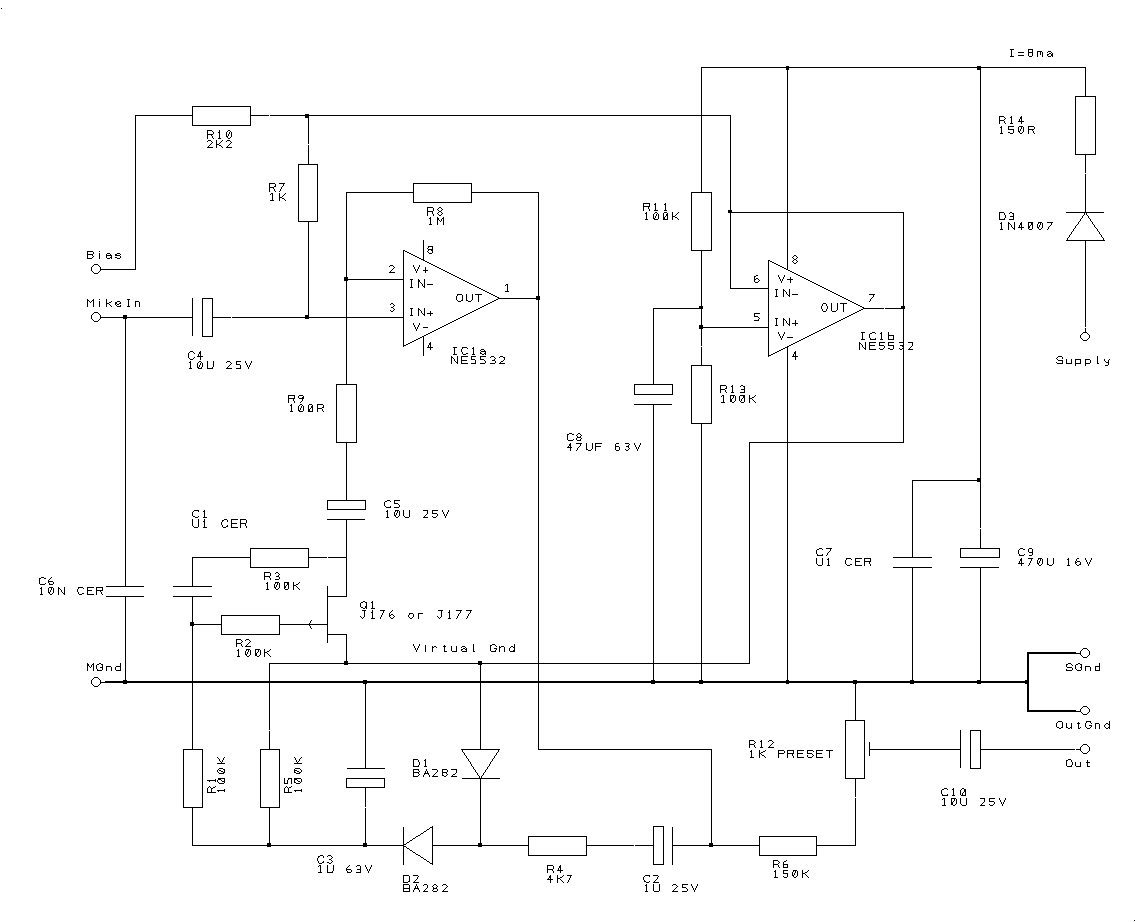
This design is not totally original with elements previously being used elsewhere1, but it does provide a cost-effective alternative to the Plessey solution. Figure 1 shows the circuit diagram, IC1a amplifies the incoming microphone signal with the gain set by R8 and the combination of R9 and the drain / source resistance of Q1.
Minimum negative feedback hence maximum gain occurs when Q1 is at minimum resistance. The output from IC1a at pin 1 is applied to the voltage doubler circuit of C2, D1, D2 and smoothing capacitor C3. This feedback voltage is applied to the gate of Q1. Minimum source to drain resistance occurs when the gate is at (or below) the source potential, as the op amp AC output increases Q1`s gate DC voltage also increases so increasing it`s resistance and decreasing gain.
At a gate to source voltage of about 2. 5V equilibrium is met where any increase in input to the op amp produces an equal reduction in gain I. E. automatic gain control. An appropriate microphone signal for the transceiver is obtained by potting down output of IC1a by R6 and R12.
IC1b is wired as a unity gain (buffer) amplifier with it`s output voltage set at ½ the supply voltage by R11 and R13, C8 provides smoothing with a long time constant. IC1b therefore provides a virtual ground, this is used to bias IC1a correctly and provide a relatively noise free bias for an electret microphone if required.
To keep the component count as low as possible and to avoid a large voltage drop no regulator has been used, the circuit of R14 and C9 provides supply smoothing assisted by D3. The primary function of this diode is to protect the op amp from the hostile vehicle electrics, voltage spikes of ±100 Volts or more are not uncommon in a car due to the switching of heavy inductive loads.
As the component count is low the circuit can quite easily be built onto a piece of strip board, I have designed a PCB for a more compact designFor D1 and D2 its best to use shotky diodes although 1N4148 types will work. The FET is a P channel junction type although by reversing the polarity of D1, D2 and C3 an N channel type may be used.
Other components aren`t critical although it is advisable to use an NE5532 for IC1, this dual op amp has a very high gain / bandwidth product of 10MHz which is matched by few other devices. The best place to fit this module is within the radio itself, as it`s still useful if hands free isn`t being used and the case will give protection against large RF fields from the antenna.
If used with a commercial transceiver though it`s unlikely that there will be enough room so the module will have to be fitted in it`s own box. If made into a self contained unit I would recommend that the earth (negative supply) be made by the ground connection to the transceiver, this way an eart
🔗 External reference
Related Circuits

The ZN416E can be configured as a simple 455-kHz IF amplifier. In this case, the circuit's center frequency and bandwidth are set by RES1, which is a Murata CSB455E ceramic resonator. The ZN416E is a versatile integrated circuit designed specifically...
This video demonstrates the fundamentals of operational amplifiers (op amps) and includes an example circuit that amplifies a small microphone signal to make it audible through earbuds. The circuit utilizes the LM324 quad op amp integrated circuit (IC). The described...
Amplifiers that operate on 12V DC typically do not deliver significant power and are often not classified as high-fidelity (hifi) devices. However, this compact stereo amplifier meets the power requirements effectively. This compact stereo amplifier is designed to operate efficiently...
This article discusses various Teralab Electronics projects involving the 2N2222 transistor. The content is straightforward and informative. The components mentioned can enhance understanding of the projects detailed in this article. For instance, readers can find and purchase the 2N2222...
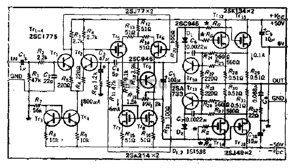
The circuit consists of three identical basic stages, with the second stage featuring a differential output from the power MOSFET, 2SJ77. A current mirror circuit utilizing 2SK214 is implemented. The operating current is 6mA; however, due to the power...
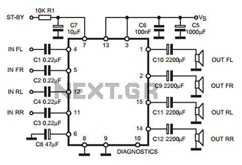
The following circuit illustrates a 35W quadruple amplifier and a 2 x 25W bridge amplifier based on the TDA7375 integrated circuit (IC). This circuit requires a minimal number of external components. Although initially designed for car applications, it can...