
MOSFETs IN SERIES
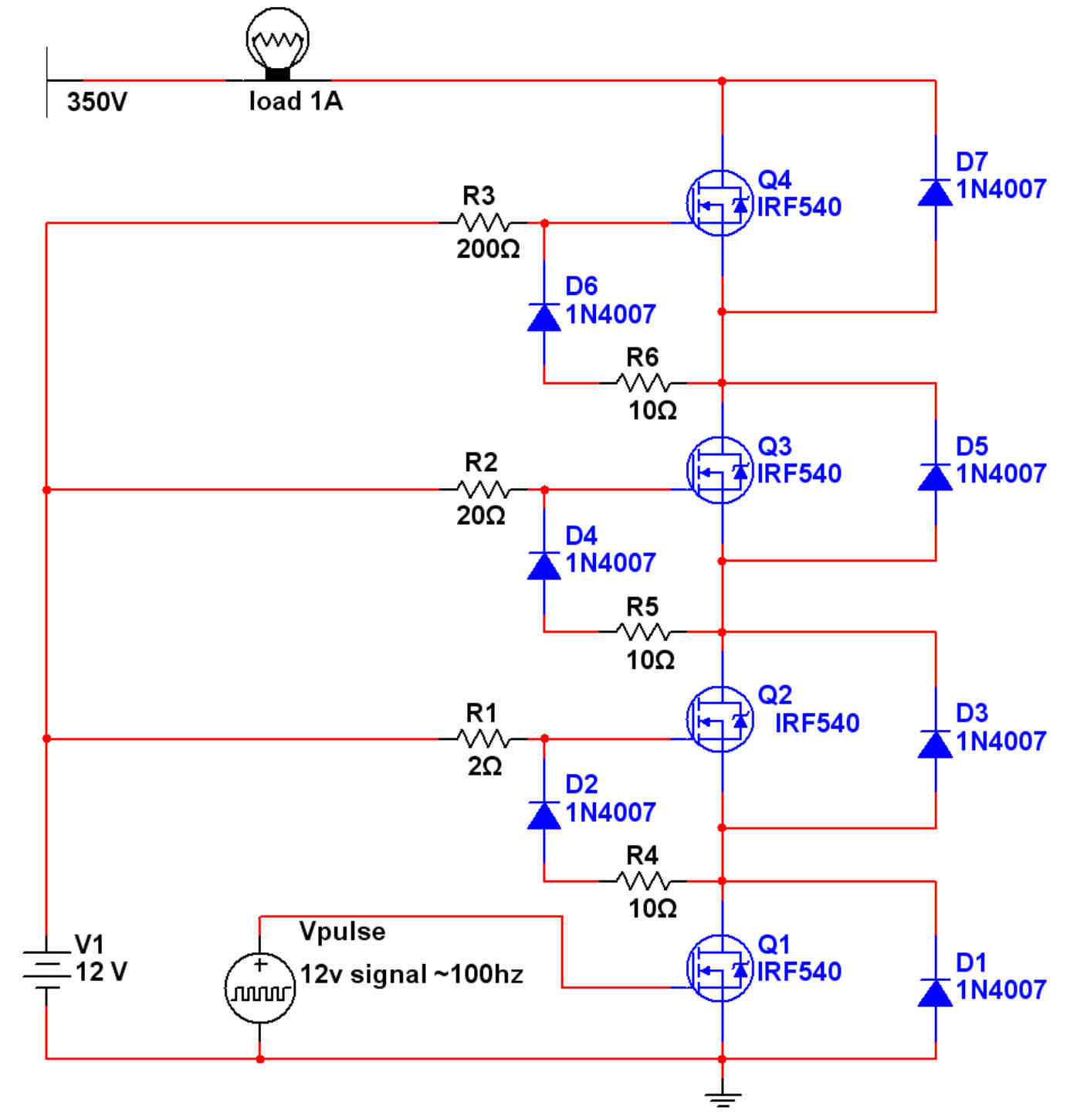
When designing a circuit that utilizes multiple MOSFETs in series for voltage amplification, it is crucial to ensure that each MOSFET operates within its specified parameters. The primary goal is to achieve a reliable switching mechanism across all MOSFETs while maintaining proper voltage levels at each gate.
The proposed circuit configuration should include a dedicated diode connected from the +12V supply to each MOSFET gate. This diode serves to isolate the gate voltage and prevent backflow, ensuring that each MOSFET receives the appropriate gate drive voltage. The use of Zener diodes between the gate and source of each MOSFET is recommended to protect against over-voltage conditions that could lead to gate damage.
In this configuration, it is essential to monitor the gate-source voltage (Vgs) and drain-source voltage (Vds) for each MOSFET. The gate-source voltage should remain within the manufacturer's specifications, typically between 10V to 20V for optimal switching. The drain-source voltage must also be carefully managed to prevent exceeding the maximum ratings, especially when cascading multiple MOSFETs, as the cumulative voltage can approach or exceed the rated limits.
Additionally, a thorough verification of the circuit connections is necessary to rule out wiring errors. Each MOSFET's terminals should be checked for correct orientation and proper connections to the power supply and load. If the fourth MOSFET remains inactive, it is advisable to measure the voltages present at the gate, source, and drain terminals of all MOSFETs to identify any discrepancies.
Safety precautions are paramount when working with high voltages. An isolating transformer should be employed to minimize the risk of electric shock, and all components should be rated for the maximum expected voltages. Furthermore, it is advisable to employ proper personal protective equipment and to work in a controlled environment to mitigate any risks associated with high-voltage circuits.A while ago i run across this document which apparently tells how to wire mosfets in series to get higher voltages (pg 10-14). This is the only schematic i found so far that is actually working. The problem is that i can`t make more than 3 mosfets work, when i add a fourth ( with the same circuitry) it remains OFF no matter what.
I tried different resistor values. At first i though that if R2 has 2ohms and R3 20ohms that the next should be 200ohms. When it didn`t work i tried 20, 50 and 1k but with no luck. Can you please tell me what i did wrong You need to post your circuit and indicate voltages used, I would suggest looking at the voltage V3 mentioned in the paper relative to V1. I wouldn`t really expect there to be a resistor value problem with this circuit. I don`t think your circuit will work. You`ve omitted the diode from the 12VDC supply to the MOSFET gates. I would use an individual diode from the +12V supply to each gate, and I would replace the gate-source diodes with zeners to protect the gate.
Then I think it would work. But why are you doing this MOSFETs that can switch 350V are readily available. Hey i`m no expert but isn`t it a "protection" matter i may do it so not to blow up anything, but the problem is that i can`t make Q4 even switch on, thats why i stripped everything out to try it as the paper suggests. Hey i`m no expert but isn`t it a "protection" matter i may do it so not to blow up anything, but the problem is that i can`t make Q4 even switch on, thats why i stripped everything out to try it as the paper suggests.
Oh sorry. I foolishly thought that it would be helpful and important to prevent you from blowing up your MOSFETs. Of course, you can just add the zeners later, if you can be bothered. If you make the changes I have suggested (diode to each gate, and zeners from gates to sources), and the MOSFETs remain OFF when +12V is applied to the gate of the bottom one, either you`ve wired something wrong, or you have a damaged MOSFET.
If you can`t find the problem, post the voltages on all three terminals of each MOSFET. Looking more closely at this, I would be careful about exceeding Vdg for these mosfets. Whilst not often specified (but can be assumed to be Vds + Vgs), it is something you need to be careful about. This is especially true when all your slave mosfets gave their gates at essentially the same potential.
If you make the changes I have suggested (diode to each gate, and zeners from gates to sources), and the MOSFETs remain OFF when +12V is applied to the gate of the bottom one, either you`ve wired something wrong, or you have a damaged MOSFET. If you can`t find the problem, post the voltages on all three terminals of each MOSFET. Looking more closely at this, I would be careful about exceeding Vdg for these mosfets. Whilst not often specified (but can be assumed to be Vds + Vgs), it is something you need to be careful about.
This is especially true when all your slave mosfets gave their gates at essentially the same potential. Don`t worry that`s probably isn`t going to happen. I work with my left hand in the pocket, and i have a transformer and a fuse so even if i get a shock (don`t think so) it won`t be lethal.
Well. if you know of any other precaution i could take it would be good. Don`t worry that`s probably isn`t going to happen. I work with my left hand in the pocket, and i have a transformer and a fuse so even if i get a shock (don`t think so) it won`t be lethal. Well. if you know of any other precaution i could take it would be good. Do a Google search. A thorough one. And when you`re working with voltages of 500V or more, a transformer (I assume you mean an isolating transformer) may not help you.
And a fuse is no use at all - they`re there to prevent fires, not electrocution. 🔗 External reference
Related Circuits

This page focuses on radios marketed in the USA, compiled by residents familiar with these products. Contributions regarding non-USA radios are welcome, and a region-specific page could be created. The MaxTrac, Radius, and GM300 series have inspired additional radio...
A comprehensive design procedure is proposed for the development of Field-programmable/Reconfigurable Analog Integrated CMOS circuits. Instead of relying on iterative simulation steps to meet design specifications by adjusting the W/L ratios of the FETs, first-order classroom equations are utilized...

It is now possible to program microcontrollers at home with a cost-effective AT89S51 series microcontroller burning IC kit. The AT89Sxx series ICs feature an inbuilt ISP (In-System Programming) module, allowing for easy programming of the microcontroller. This document presents...

JG series of photoelectric relay circuit. To ensure reliable operation, a Schmitt trigger circuit has been incorporated. These circuits function similarly; when light strikes the photosensitive component, its internal resistance decreases, activating the transistor VT and subsequently energizing the...
Diode D1 and resistor R1 provide VDD isolation during the programming of 24-pin devices. Jumper J3 must be shorted for 24-pin devices and left open for programming 28-pin devices. The following EEPROMs are pin compatible with their EPROM versions. In...
Pre-amplifiers utilize a tandem-type current feedback circuit, with an output impedance that is approximately equal to the DC collector resistance (Rc). The input impedance of the RC attenuator is equivalent to the load impedance of the amplifier. In the...