
MSP430 Ultra-Low Power 16-bit Microcontroller
1) Yes, J3 and J6 are pin connectors with named signals on them. If a Bill of Materials (BOM) is available for this schematic, it may list package information. However, these are likely just breakout pins. 2) Yes, the chip likely has multiple VCC/GND pins. Many higher-integrated chips include additional pins to facilitate easier bonding and to prevent voltage drops due to higher currents through thin internal bonding. 3) Yes, the layout of the crystal is critical. It is advisable to avoid placing anything near the crystal and its connections to the chip that could create parasitic capacitances or signals that may crosstalk to or from the crystal. Before posting bug reports or seeking assistance, it is recommended to conduct a quick scan of relevant articles, as these apply to any problem reporting on forums. If discussing the issue publicly is not feasible, starting a private conversation is an option, although public threads are preferred for broader benefit. All content and materials on this site are provided "as is," with no representations about their suitability for any purpose, and all warranties are disclaimed. Use of the information may require a license from a third party or TI, and all postings are subject to the site's Terms of Use.
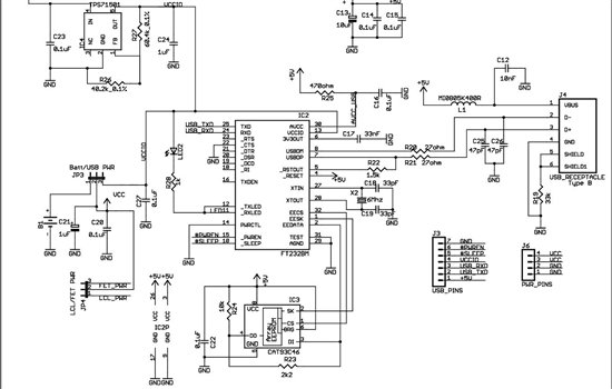
The USB schematic for the pulse oximeter application outlined in SLAA458 serves as a crucial interface for data transmission from the pulse oximeter to a host system. The FT232BM chip utilized in this design is a versatile USB to serial converter, enabling effective communication between the pulse oximeter and a computer or microcontroller. The connections labeled J3 and J6 are likely designated for specific signal routing, serving as breakout headers that facilitate the connection of additional components or peripherals to the FT232BM.
In the schematic, the lower left connections labeled IC2P indicate specific power requirements for various pins of the FT232BM. The presence of multiple VCC and GND pins is typical for integrated circuits, allowing for improved current distribution and reduced voltage drop across the chip. This design consideration is critical in applications where power integrity is paramount, especially in high-frequency or high-current scenarios.
The layout of the crystal oscillator in the design is also a vital aspect, as it influences the overall stability and performance of the clock signal. Proper placement is essential to minimize parasitic capacitance and avoid crosstalk, which can adversely affect the oscillator's performance. Following best practices in PCB design, such as maintaining adequate spacing from noisy signals and ensuring a solid ground plane, will enhance the reliability of the pulse oximeter's operation.
Overall, this schematic provides a foundation for understanding the electrical connections and operational requirements of the pulse oximeter application, ensuring that data can be accurately collected and transmitted through the USB interface.As found in SLAA458, the revised pulseoximeter application, I`ve attached an image of the USB schematic that is used to output collected data. I just had a few questions about this schematic. 1) What do J3 and J6 correspond to I can see the corresponding node names on the Ft232BM chip on J3, but these two are not present in any other schematic of
the project. Is this simply a 7-pin header used to tidily connect components to the chip 2) In the lower left hand side of the schematic, there are two connections labeled IC2P with pin numbers going from ground or vcc. Does this simply mean pins 26 and 3 need vcc while pins 17 and 9 need to be grounded 1) Yes, J3 and J6 are just pin connectors with the named signals on them.
If you have a BOM for this schematic, it may list package information. But most likely these are just breakout pins. 2) Yes. The chip likely has more than one VCC/GND pin. Many higher-integrated chips have, to allow easier bonding inside. Or to prevent voltage drops because of higher currents through the thin internal bonding. 3) Yes again. Crystal layout is a difficult thing. There are soem threads abotu this in this forum. Basically: avaoid anything near teh crystal and its connections to the chip that can form parasitic (and even more unbalanced parasitic) capacitances, as well as signals that can crosstalk to (or from) the crystal. Before posting bug reports or ask for help, do at least quick scan over this article. It applies to any kind of problem reporting. On any forum. And/or look here. If you cannot discuss your problem in the public, feel free to start a private conversation: click on my name and then `start conversation`.
But please do so only if you really cannot do it in a public thread, as I usually read all threads. And I prefer to answer where others can profit from it (or contribute to it) too. All content and materials on this site are provided "as is". TI and its respective suppliers and providers of content make no representations about the suitability of these materials for any purpose and disclaim all warranties and conditions with regard to these materials, including but not limited to all implied warranties and conditions of merchantability, fitness for a particular purpose, title and non-infringement of any third party intellectual property right. TI and its respective suppliers and providers of content make no representations about the suitability of these materials for any purpose and disclaim all warranties and conditions with respect to these materials.
No license, either express or implied, by estoppel or otherwise, is granted by TI. Use of the information on this site may require a license from a third party, or a license from TI. Content on this site may contain or be subject to specific guidelines or limitations on use. All postings and use of the content on this site are subject to the Terms of Use of the site; third parties using this content agree to abide by any limitations or guidelines and to comply with the Terms of Use of this site. TI, its suppliers and providers of content reserve the right to make corrections, deletions, modifications, enhancements, improvements and other changes to the content and materials, its products, programs and services at any time or to move or discontinue any content, products, programs, or services without notice.
🔗 External reference
Related Circuits
This application note discusses the use of SEPIC power modules to supply the necessary power for driving high-brightness LED arrays. These arrays serve as display backlights and necessitate a wide dimming range. The SEPIC configuration offers an efficient and...
Integration of 1200V SOI gate driver ICs into a medium power IGBT module package. A novel approach for medium power applications. The integration of 1200V Silicon-On-Insulator (SOI) gate driver Integrated Circuits (ICs) into medium power Insulated Gate Bipolar Transistor (IGBT)...
The following diagram illustrates a 50W offline switching power supply circuit design. This circuit is powered by a MOSFET, specifically the BUZ80A/IXTP4N8 for a 220V AC voltage input and the GE IRF823 for a 110V AC voltage input. The...
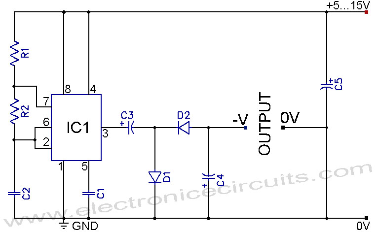
A 555 negative voltage power supply circuit can be created using a charge-pump configuration that incorporates a 555 timer, diodes, and additional components. The 555 timer is a versatile integrated circuit commonly used in various applications, including oscillators, timers, and...
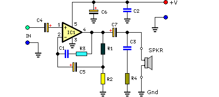
This compact amplifier is built around the TDA2003 integrated circuit, which can deliver 4W RMS at a 4-ohm load. The TDA2003 offers enhanced performance while maintaining the same pin configuration as the TDA2002. It retains the advantageous features of...

More: A comprehensive electronic schematic that outlines the design and functionality of a specific circuit is crucial for understanding its operation. The schematic should include components such as resistors, capacitors, diodes, transistors, and integrated circuits, along with their interconnections....