
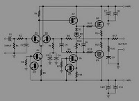
OCL yourself feedback amplifier analysis
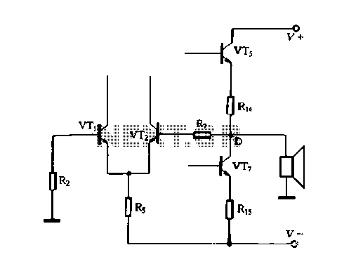
In this DC feedback circuit, the key component is the resistor R7, which plays a crucial role in establishing the feedback loop. By connecting R7 to the output terminal, it allows the circuit to sense the output voltage and adjust the input accordingly. The differential input stage is designed to amplify the input signal while maintaining stability through negative feedback. The voltage follower configuration ensures that the output voltage closely follows the input voltage, providing a high input impedance and low output impedance.
The gain of the circuit is set to 10, which means that for every 1 volt change at the input, the output will change by 10 volts. This gain is achieved through the careful selection of the feedback components and the operational amplifier used in the circuit. The operational amplifier's properties, combined with the feedback from R7, ensure that the output remains stable and responsive to changes in the input.
The midpoint voltage VD is critical for the operation of the circuit. When VD is at zero volts, the circuit operates in its desired state. However, if external factors cause VD to increase, the feedback loop will detect this change. The operational amplifier will respond by adjusting the input, effectively reducing VD back to its nominal value of zero volts. This self-regulating feature is essential for maintaining the performance of the circuit under varying conditions.
Overall, this DC feedback circuit exemplifies the principles of negative feedback in electronic design, showcasing how simple components can work together to create a stable and effective voltage follower. The design ensures that the output remains consistent and reliable, providing a robust solution for applications requiring precise voltage tracking.DC feedback works shown in Figure l-31. In the circuit, R7 connected to the output terminal (the midpoint of static) D of the differential input stage Vr, between the base. Sta tic, this is a whole negative feedback circuit, which is a voltage follower, the voltage at a magnification of 10 output voltage follows the input voltage changes o As previously analyzed, Vbl VbZ ov, so the midpoint voltage VD OVo when some reason the VD increases, the negative feedback regulation, will automatically make the VD word back ovo
Related Circuits

The TDA 2030 is a widely used 14W audio power amplifier monolithic integrated circuit in a Pentawatt package, intended for use as a low-frequency Class AB amplifier. Some home theater prototypes utilize the TDA 2030 as a low-frequency subwoofer...
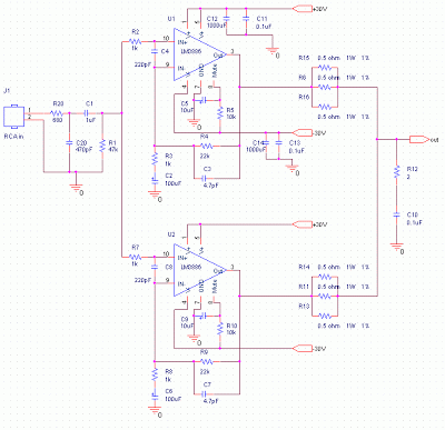
This audio amplifier design employs two LM3886 chips per channel in a parallel configuration, based on the PA100 parallel amplifier detailed in National Semiconductor's application note AN1192. It can deliver approximately 50W into an 8-ohm speaker and 100W into...
A friend is interested in building a hi-fi power amplifier, specifically a Class AB model due to its quality sound, particularly in bass response and distinct clarity. This circuit is designed as a hi-fi OCL (Output Capacitor-Less) power amplifier...
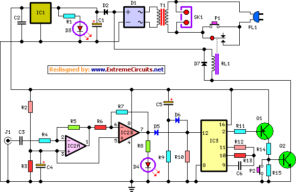
This circuit deactivates an amplifier or any connected device when a low-level audio signal at its input is absent for at least 15 minutes. By pressing P1, the device is powered on, supplying power to any appliance connected to...
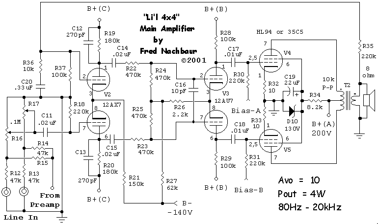
The supply voltage rails were conservatively maintained at +40V and -40V. For those interested in experimentation, the supply voltage can be increased to a maximum of +50V and -50V, enabling the amplifier to reach its target output of 100W...
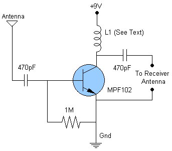
This schematic illustrates an FM, AM/MW, and SW antenna amplifier circuit, also referred to as an antenna preamplifier circuit. It is designed to enhance weak signals from FM, AM/MW, and SW bands. The circuit is straightforward and can be...
Warning: include(partials/cookie-banner.php): Failed to open stream: Permission denied in /var/www/html/nextgr/view-circuit.php on line 713
Warning: include(): Failed opening 'partials/cookie-banner.php' for inclusion (include_path='.:/usr/share/php') in /var/www/html/nextgr/view-circuit.php on line 713