
On After Delay with Mosfet
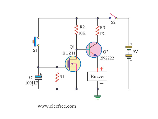
The On After Delay Circuit is designed to provide a delay in the activation of a load after a switch is pressed. The core component of this circuit is a MOSFET, which is preferred over a traditional bipolar junction transistor (BJT) due to its efficiency and ease of use in delay applications.
When switch S1 is pressed, it initiates the delay mechanism. The circuit typically includes a resistor-capacitor (RC) timing network that determines the length of the delay. The capacitor charges through the resistor when S1 is activated, and the voltage across the capacitor rises gradually. Once the voltage reaches a certain threshold, the MOSFET turns on, allowing current to flow to the load.
The MOSFET's gate is connected to the junction of the resistor and capacitor, ensuring that it remains off until the capacitor's voltage is sufficient to exceed the gate-source threshold voltage. This arrangement provides a reliable and adjustable delay, which can be modified by changing the values of the resistor and capacitor.
To ensure proper operation, it is important to select a MOSFET with suitable specifications for the load current and voltage. Additionally, the circuit can incorporate a pull-down resistor to ensure that the MOSFET remains off when S1 is not pressed, preventing false triggering due to noise or floating voltages.
Overall, this On After Delay Circuit is a versatile solution for applications requiring delayed activation, such as in lighting systems, alarms, or other electronic devices where a time delay is beneficial.That be On After Delay Circuit. I uses mosfet in the circuit for delay easy more than the transistor. By have the work of the circuit be when press , S1 ,. 🔗 External reference
Related Circuits
This basic MOSFET amplifier is simple to construct and low-cost, making it ideal for Hi-Fi amplifiers and instrument amplifiers such as guitars and keyboards. It delivers an output power of ±100 W RMS at an 8-ohm load or ±160...
This circuit is a simple connection delay lamp circuit. When the lights are turned on and the switch is pressed, the power supply is activated. The capacitor charges rapidly, causing the thyristor (VT) to open, which in turn lights...
555 Timer with On-Off Delay Circuit. This circuit utilizes the commonly available 555 integrated circuit (IC) to create a timer that allows for time adjustment in both on and off states. The 555 timer is a versatile device widely used...
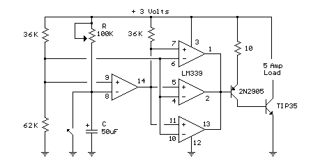
In this circuit, an LM339 quad voltage comparator is used to generate a time delay and control a high current output at low voltage. Approximately 5 amps of current can be obtained using a couple of fresh alkaline D...
The circuit integrates several functions, including a smooth startup for the AC power line, with a one-second delay before connecting to the power supply transformers of the amplifier through relay RL1 and resistor Rx. This delay is designed to...
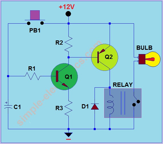
This circuit operates by activating a headlight when the push-button PB1 is pressed. The headlight remains illuminated for a predetermined duration, which can range from several seconds to minutes, before automatically turning off. When PB1 is engaged, capacitor C1...