
Pierce oscillator
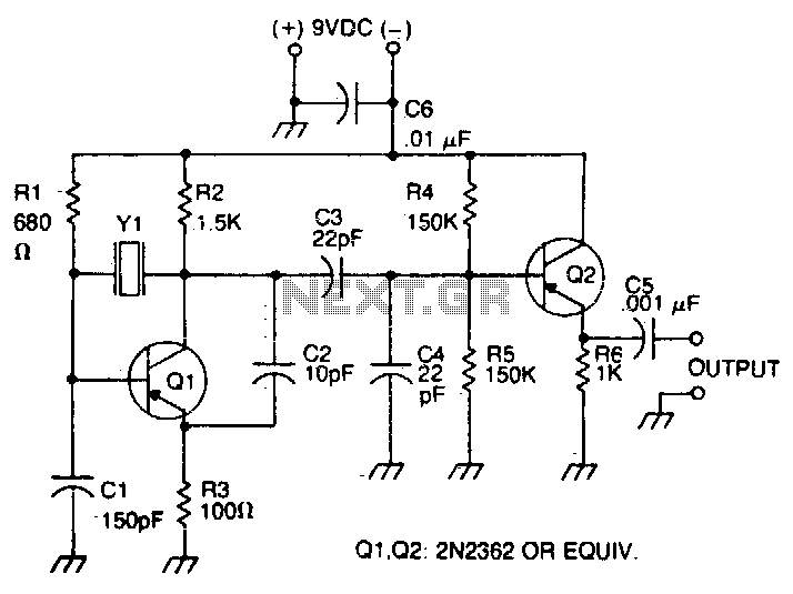
The circuit described features an oscillator configuration utilizing a transistor (Q1) in conjunction with a crystal for frequency stabilization. The crystal is strategically positioned between the collector and base of Q1, which facilitates the generation of oscillations at a precise frequency determined by the characteristics of the crystal. This setup is typical in oscillator circuits where stability and accuracy are paramount.
To enhance feedback within the circuit, a capacitor (C2) is connected across the collector-emitter junction of Q1. This capacitor plays a critical role in shaping the feedback loop, ensuring that the oscillations are sustained and stable. The inclusion of C2 allows for better control over the phase shift and gain, contributing to improved performance of the oscillator.
Additionally, transistor Q2 serves as an output buffer. This component is essential for isolating the oscillator stage from subsequent circuitry, thereby preventing loading effects that could dampen the oscillations. The output buffer allows for a stronger drive capability, enabling the oscillator to interface effectively with other components or stages of the circuit without compromising the integrity of the oscillation signal.
Overall, this configuration exemplifies a common approach in electronic oscillator design, where stability, feedback control, and output buffering are critical considerations for successful operation.The oscillator transistor is Ql, and the crystal is placed between the collector and base. Feedback is improved by the use of the collector-emitter capacitor C2 Transistor Q2 is used as an output buffer. 🔗 External reference
Related Circuits
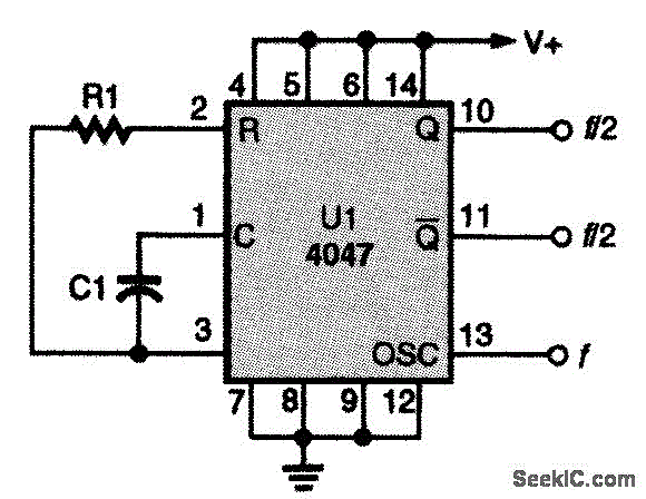
This CMOS square-wave oscillator utilizes the 4047 multivibrator circuit, suitable for both monostable (one-shot) and astable applications. In the provided configuration, the 4047 operates as an astable multivibrator. The circuit features three outputs from the 4047, with the first...
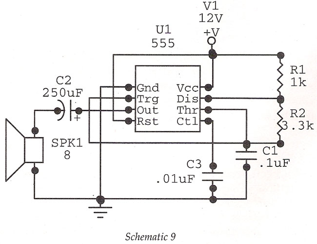
Basic Oscillator (Tone Generator) at 1.8 kHz using IC 555. This circuit features an astable oscillator configuration built around the 555 timer IC, generating an alarm tone of 1.8 kHz that directly drives a speaker. This is a fundamental...
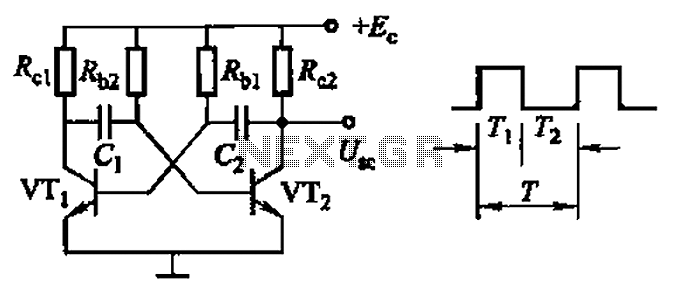
Common non-sinusoidal oscillator circuit, waveform and frequency formula - square wave oscillator - self-excited multivibrator The common non-sinusoidal oscillator circuit, specifically the square wave oscillator, is a fundamental electronic circuit utilized to generate square wave signals. It operates based on...
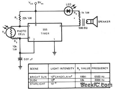
This circuit's frequency of oscillation increases directly with light intensity. The greater the light intensity, the higher the frequency of the oscillator. The 555 timer operates in astable oscillator mode, where frequency and duty cycle are controlled by two...
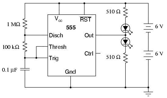
The 555 integrated circuit is a versatile timer that can be used for various applications. This experiment focuses on its operation as an astable multivibrator or oscillator. When connected to a capacitor and two resistors, it generates a square-wave...
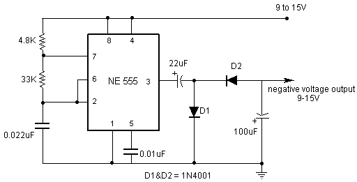
The square wave oscillator does not necessarily need to be a 555 timer; it can also be implemented using a ring oscillator with inverters. However, when utilizing 4000 series CMOS logic, the negative output voltage generated may have limited...