
pll fm demodulator

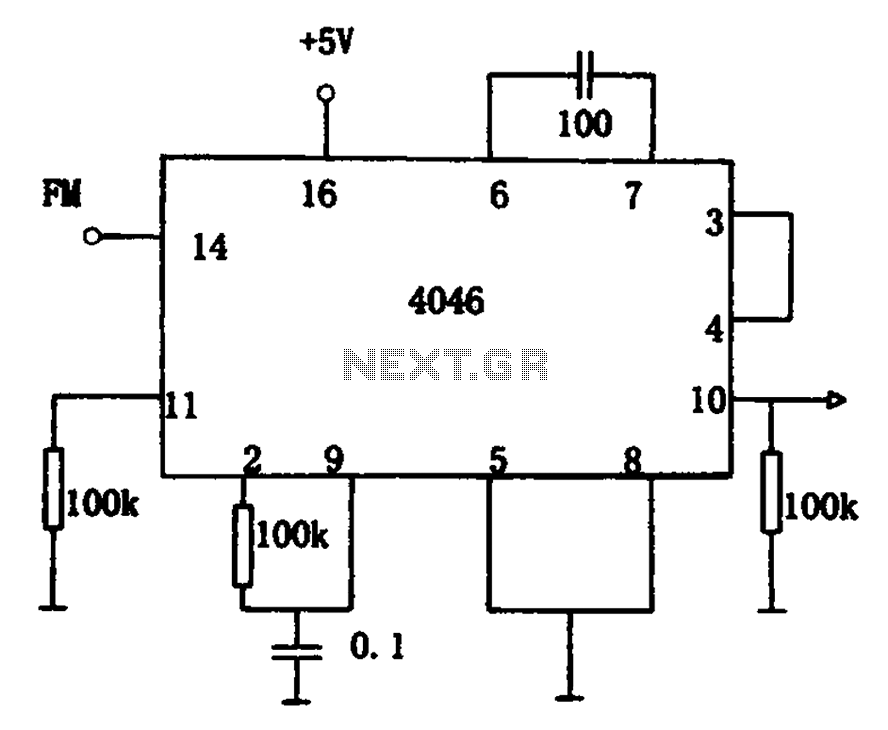
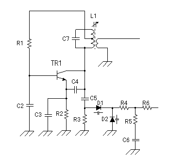
The FM demodulator circuit utilizing the CD4046B PLL integrates a VCO, phase comparator, and feedback loop to achieve demodulation of frequency-modulated signals. The VCO generates a frequency output that is adjusted based on the input voltage, which corresponds to the frequency of the incoming FM signal. In this setup, the 10 kHz carrier frequency is effectively tracked by the VCO, enabling the extraction of the modulating 400 Hz audio signal.
AC coupling is implemented at the input to ensure that only the varying component of the FM signal is processed, blocking any DC offset that may interfere with the demodulation process. The choice of Phase Comparator I is critical as it allows for the comparison of the phase of the VCO output with the incoming FM signal. This phase comparison is essential for maintaining lock and ensuring that the VCO output remains synchronized with the carrier frequency of the FM signal.
The circuit's design leverages the high signal-input-noise-rejection capabilities of Phase Comparator I, which enhances the overall performance of the demodulator by minimizing the impact of noise on the demodulated output. As a result, this PLL-based FM demodulator is suitable for various applications where reliable demodulation of FM signals is required, such as in radio receivers and communication systems. The schematic provides a clear representation of the connections and components involved, facilitating understanding and implementation of the circuit in practical applications.This is a circuit about PLL system that can be used to implement an FM demodulator. Since the VCO output tracks the FM signal, and the VCO input voltage is proportional to the VCO output frequency, then the VCO input will be equal to the demodulated signal. This is the figure of the circuit. For this example, an FM signal consisting of a 10-kHz ca rrier frequency was modulated by a 400-Hz audio signal. The schematic diagram shows the connections of the CD4046B as an FM demodulator. The total FM signal amplitude is 500 mV, therefore, the signal must be ac coupled to the signal input (terminal 14). Phase comparator I is used for this application because a PLL system with a center frequency equal to the FM carrier frequency is needed.
Phase comparator I lends itself to this application also because of its high signal-input-noise-rejection characteristics. 🔗 External reference
Related Circuits
The circuit utilizes the 4046 Phase-Locked Loop (PLL) for FM demodulation, incorporating an intermediate frequency (IF) FM demodulation output based on the input signal frequency. The 4046 PLL is a versatile integrated circuit that can be configured for various applications,...
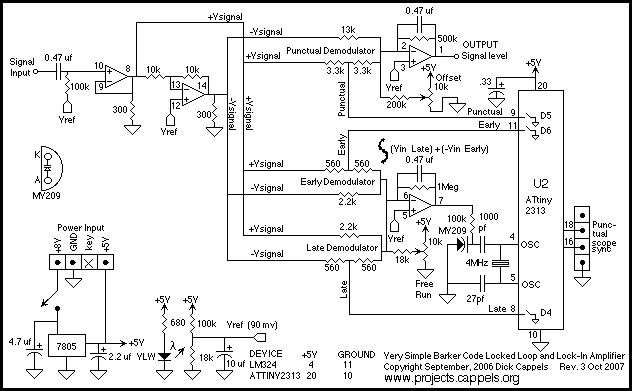
A simple, low component count phase locked loop that locks onto and detects the amplitude of an incoming baseband 7 bit Barker code using a switched resistor demodulator that is driven directly by a microcontroller's output pins. Balanced modulators...
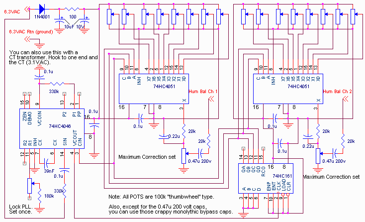
This report outlines the operation and adjustment of a Phase Locked Loop (PLL) hum cancellation circuit designed to reduce residual hum from amplifiers. This circuit is particularly useful for Directly Heated Triode (DHT) amplifiers with AC-operated filaments, where a...
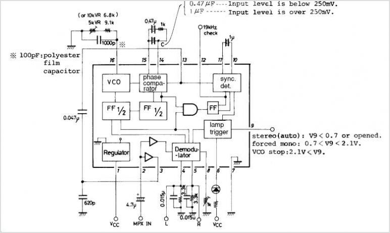
The LA3370 is a multiplex integrated circuit (IC) designed for FM car stereo applications. It performs two primary functions using the intermediate frequency (IF) meter output voltage: 1. Stereo Noise Control (SNC), which effectively reduces noise specific to FM...
The output frequency can be altered based on the division ratio of the comparison frequency in the 10 kHz unit, with the division ratio set to 1024 in this circuit. Given that the amateur radio bandwidth in Japan is...
The ADM1066 is a configurable supervisory and sequencing device that provides a single-chip solution for supply monitoring and sequencing in systems with multiple power supplies. In addition to these capabilities, the ADM1066 features a 12-bit ADC and six 8-bit...