
Power-line-modem
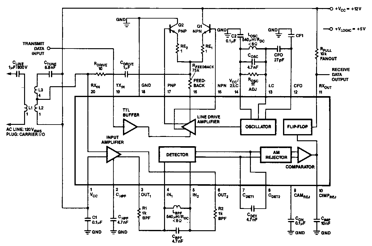
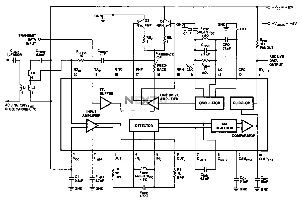
In the 100 kHz application, the coupling network connects to the receiver section located at the bottom of the chip. The external components will be summarized later. The receive data output is pulled up through a resistor (RPuLL) valued at approximately 10 kΩ. A minimum current of 10 mA establishes the voltage drop across RPuLL. An additional voltage supply, VLoGJc, is available for users who wish to output data at TTL levels. The transmitter section is positioned at the top, with the oscillator network and the class configuration extending from right to left.
The circuit operates at a frequency of 100 kHz, utilizing a coupling network that effectively interfaces with the receiver section of the integrated circuit. This network is critical for ensuring that the signals are transmitted with minimal distortion and maximum fidelity. The receiver section is designed to interpret the incoming signals, and the output is configured to pull up through a resistor (RPuLL) of approximately 10 kΩ. This resistor plays a significant role in setting the logic levels of the received data, ensuring that the output is compatible with subsequent processing stages.
The current flowing through RPuLL is maintained at a minimum of 10 mA, which is essential for establishing a sufficient voltage drop across the resistor, thereby providing a reliable high logic level for digital communication. The presence of an additional voltage supply, labeled VLoGJc, allows for the flexibility of outputting signals at TTL (Transistor-Transistor Logic) levels, which is a standard voltage level for digital circuits, ensuring compatibility with various digital systems.
The transmitter section, located at the top of the chip, includes an oscillator network designed to generate the necessary carrier frequency for data transmission. This section is crucial for modulating the data signal onto the carrier wave, allowing for effective wireless communication. The design of the transmitter and receiver sections is integral to the overall functionality of the circuit, ensuring efficient data transfer and reception while maintaining signal integrity across the specified operating frequency.In the 100-kHz application from left to right, the coupling network feeds into the receiver ~section on the bottom of the chip. (The external components are summarized later.) The receive data output is pulled up via RPuLL ~ 10 K!l.
A minimum current of 10 mA sets the voltage drop across RpuLL?? Another voltage supply, VLoGJc, is shown if the user wants to have the output sent at TTL levels. Across the top is the transmitter section; going from right to left, the oscillator network, the clas. 🔗 External reference
Related Circuits
In the 100-kHz application, the coupling network feeds into the receiver section located at the bottom of the chip. The external components are summarized later. The receive data output is pulled up via a resistor (RPuLL) of approximately 10...