
Programmable gain amplifier
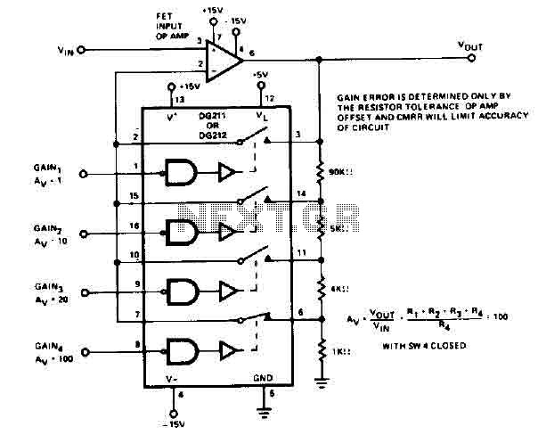
The circuit is designed around the DG212, a dual analog switch that allows for precise control over the gain of the signal. The gain configuration is established by selecting appropriate resistor values, which can be adjusted based on the desired output level. The switch SW4 is integral to this configuration, enabling the user to select different gain settings by closing the switch, thereby routing the signal through different resistor paths.
The gain error in this circuit is a critical parameter, primarily determined by the tolerance of the resistors used in conjunction with the operational amplifier's offset voltage. Resistor tolerances can introduce variability in the gain, while the offset of the op-amp can shift the entire output level. Common-mode rejection (CMR) is also essential as it impacts the circuit's ability to reject noise and interference, which is particularly important in precision applications.
In addition to the DG212, the DG211 can be utilized within the same schematic. The DG211 is similar in function but is a single analog switch, which may be beneficial in designs requiring fewer channels or for applications where space is constrained. The choice between the DG211 and DG212 will depend on the specific requirements of the circuit, such as the number of channels needed and the complexity of the gain control.
Overall, careful consideration of component selection, including resistor values and operational amplifier specifications, is necessary to achieve optimal performance in terms of gain accuracy and stability within the circuit.The circuit uses the DG212 which controlling the gain using resistors. To calculate the different gains SW4 should be closed. Gain error is determined only by the resistor tolerance op amp offset and CMR will limit accuracy of circuit. You can use the DG211 as well in the same schematic. 🔗 External reference
Related Circuits
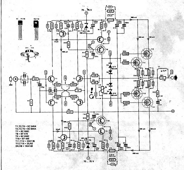
The power amplifier circuit utilizing MOSFET technology has gained significant popularity due to its aggressive sound characteristics when compared to traditional transistors and integrated circuits. It offers both low-frequency and high-frequency responses and is known for its durability. Generally,...
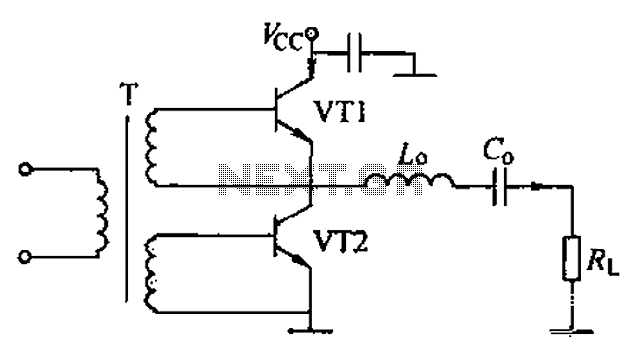
A complementary voltage switching Class D amplifier circuit is presented. Transistors VT1 and VT2 are 3DA12 types, while another transistor, VT3, is of the 3DK41C type. The collector is connected to a constant DC voltage of 12V. The input...

This amplifier delivers 20 W per channel with an input sensitivity of approximately 300 mV into a 47 kΩ load. It utilizes a bridged output configuration, allowing the speakers to be operated with both wires above ground. A +12...
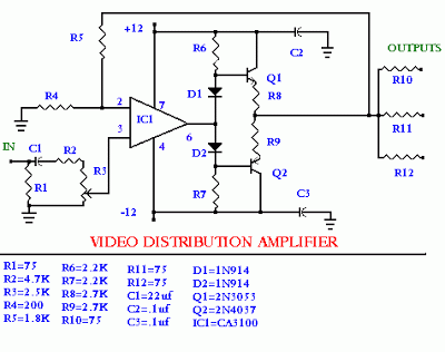
Given the variety of equipment in modern home entertainment systems, the ability to adjust the gain of both audio and video signals has become essential. This particular circuit has proven to be very useful when used alongside the General...
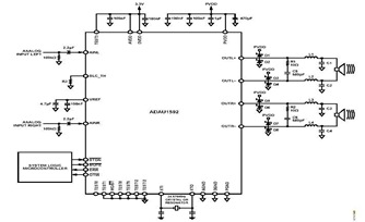
This is a typical stereo application circuit schematic of the ADAU1592, a 2-channel, bridge-tied load (BTL) switching audio power amplifier. The ADAU1592 can be utilized in flat panel televisions, PC audio systems, and mini-component applications. The ADAU1592 is designed to...
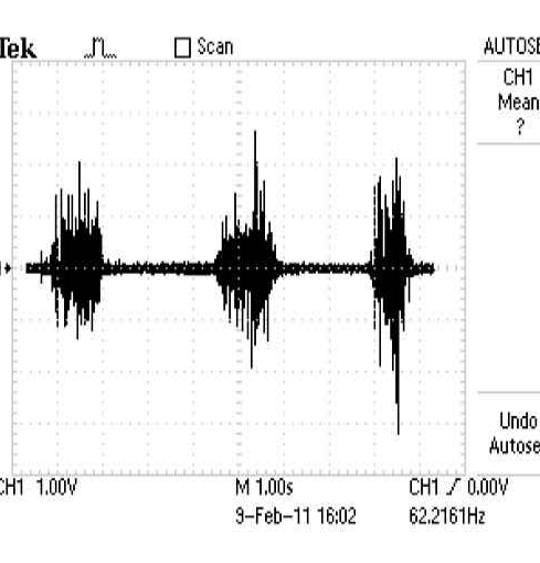
The project involves constructing two similar EMG circuits with different gain settings to measure electromyography (EMG) signals from two forearm muscles: the Flexor Digitorum Superficialis (FDS) and the Extensor Carpi Radialis Longus (ECRL). The outputs from these circuits will...