
Complementary voltage switching Class D amplifier circuit
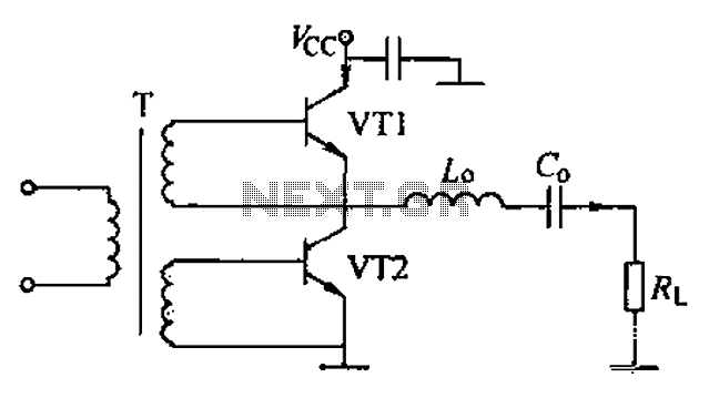
The complementary voltage switching Class D amplifier circuit operates by utilizing two NPN transistors, VT1 and VT2 (3DA12), in a push-pull configuration. This arrangement allows for efficient switching between the two transistors, enabling them to alternately conduct and cut off. The third transistor, VT3 (3DK41C), is used to enhance the circuit's performance and stability.
The circuit is powered by a constant DC voltage of 12V, which is applied to the collectors of the transistors. The input signal is coupled through a high-frequency transformer (T1), which facilitates the generation of square wave excitation voltages. When the input signal is applied, it induces a magnetic field in the transformer, producing a corresponding output voltage that drives the base terminals of VT1 and VT2.
As the input signal oscillates, one transistor turns on while the other turns off, creating an alternating current (AC) output. This switching action produces a square wave voltage across the load, which is equal to the supply voltage. The high Q factor of the circuit is instrumental in determining the fundamental frequency, allowing for selective amplification of the desired signal while minimizing distortion.
This design is particularly advantageous for applications requiring high efficiency and compact size, such as audio amplification and RF transmission. The Class D amplifier's ability to handle high power levels with minimal heat generation makes it suitable for various electronic devices. Properly implemented, this circuit can deliver high-quality audio signals with reduced power consumption. Complementary voltage switching Class D amplifier circuit shown in Fig. Transistor VT1, VT2 are 3DA12. Among them, two of the same type (NPN) tube series product transistor VT is 3DK41C. Collector plus a constant DC voltage VLr 12V: an input circuit through the high-frequency transformer Tl, so I. this tube VI. 1 and anti-VT2 get to the square wave excitation voltage. Due to increase in both series n ij Journal (NPN) transistor input terminal of the voltage is large enough and the opposite phase, two tubes in switch state and alternately turned on.
Voltage across the circuit to a square wave. Size equal to the DC supply voltage V (Jc.k, cJ series circuit composed of a high Q to select the fundamental frequency. Therefore, this amplifier is referred to as the voltage switching Class D amplifiers .
Related Circuits
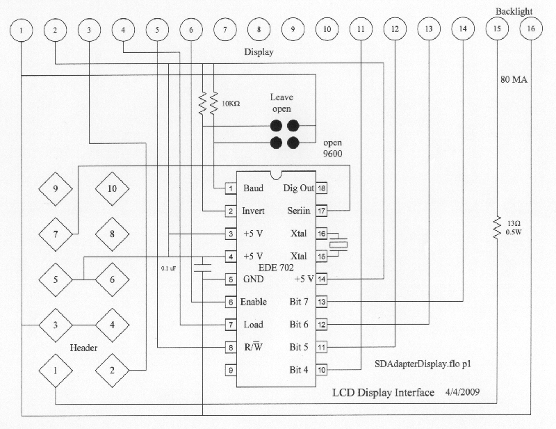
A purchase was made of the EDE702 along with an LED-backlit LCD character display. After acquiring the EDE702, it was determined that it lacked sufficient integration with HD44780-compatible displays to justify its cost. However, utilizing it was preferable to...
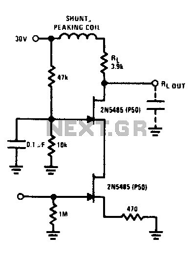
The FET cascode video amplifier exhibits very low input loading and minimizes feedback to nearly zero. The 2N5485 transistor is utilized due to its low capacitance and high transconductance (YfS). Additionally, the bandwidth of this amplifier is constrained by...
By adjusting the oscillators so their frequencies are very nearly the same, the difference between them is made audible as a beat note. This beat note changes slightly when the search loop is moved over or near to a...

All semiconductors exhibit the tendency to alter their fundamental characteristics in response to changes in ambient temperature. Basic electronic components such as transistors and diodes are particularly susceptible to variations in case temperature. The alteration in their characteristics is...
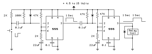
The circuit below illustrates generating a single positive pulse which is delayed relative to the trigger input time. The circuit is similar to the one above but employs two stages so that both the pulse width and delay can...
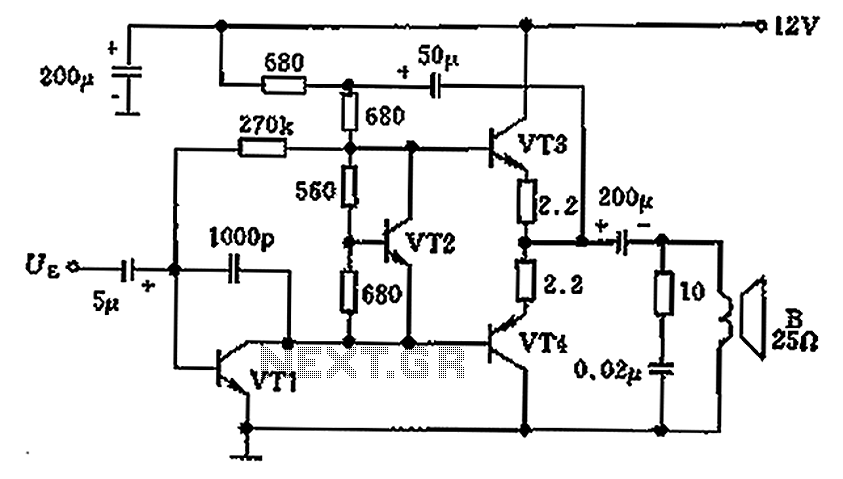
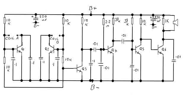
The overload protection circuit operates at a power of 650 mW with a supply voltage of 12 V and is designed for a speaker with an impedance of 25 ohms. The component specifications include: VT1 as transistor NB111EH/J, VT2...