
RC audio oscillator with 555
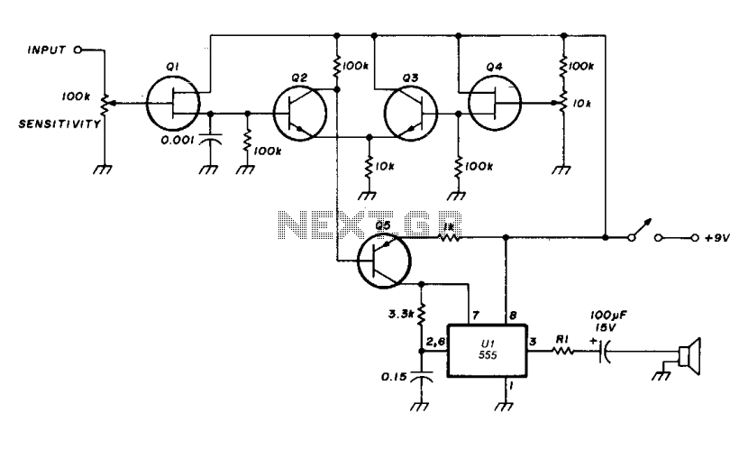
The circuit primarily involves a voltage-controlled oscillator (VCO) that utilizes a transistor (Q5) and a resistor (1000 ohms) for frequency modulation. The VCO operates by adjusting the charging current to a timing capacitor (0.15 µF), which directly influences the oscillation frequency. The forward bias applied to Q5 modulates this charging current, allowing for dynamic frequency control.
When the voltage at pins 2 and 6 of the timer IC (U1) reaches a threshold of 2A Vcc, which corresponds to approximately 6 volts in this configuration with a 9-volt power supply, the timer is triggered. This action results in pin 3 being pulled low, indicating the start of a timing cycle. Simultaneously, pin 7, configured as an open collector output, also transitions low, which initiates the discharge process of the timing capacitor through a 3.3-kilohm resistor.
The discharge time, governed by the 3.3-kilohm resistor, is crucial in shaping the output waveform of the VCO. This resistor ensures that the waveform, while asymmetrical, remains within acceptable limits for generating an aural signal. The waveform's characteristics are essential for applications that require specific frequency modulation, making this arrangement particularly useful in audio signal generation or similar applications.
Once the voltage drops to 1A Vcc, the internal flip-flop mechanism within the timer IC resets. This reset action causes pin 3 to return to a high state, while the open collector output on pin 7 becomes inactive (floats). This reset condition marks the end of the timing cycle, allowing the process to repeat, thus maintaining continuous oscillation and providing a stable output frequency for the desired application. The overall design emphasizes the importance of component selection and configuration in achieving precise control over signal generation in electronic circuits.Transistor Q5 and the 1000 ohm resistor form the variable element needed for controlling the frequency of VCO by limiting the charging current flowing into the 0.15 timing capacitor according to the forward bias being applied to Q5. As the voltage on pins 2 and 6 of Ul reach 2A Vcc (about 6 volts with a 9-volt supply) the timer will fire and pin 3 will be pulled low.
Pin 7, an open collector output, goes low and begins to discharge the timing capacitor—through the 3.3 kilohm resistor. The discharge time provided by this resistor assures a reasonable, although asymmetrical, waveform for the aural signal generated by Ul. At lA Vcc the internal flip-flop resets, the output on pin 3 goes high, the open collector output on pin 7 floats, and the timing cycle begins again.
🔗 External reference
Related Circuits
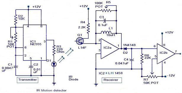
The following circuit illustrates an Infrared Motion Sensor circuit diagram. Features include the use of the NE555 integrated circuit, with a detection zone coverage of 80 degrees. The Infrared Motion Sensor circuit utilizes the NE555 timer IC configured in a...
The issue began when a girlfriend expressed her frustration with mosquitoes disrupting her nights. It was recognized that mosquito sprays provide only temporary relief, as the insects tend to return after some time. A suggestion was made for an...
The circuit was designed to operate a frequency modulation voice transmitter over the FM band within the VHF frequency range. The transmitter is an electronic device. The frequency modulation (FM) voice transmitter circuit operates within the VHF (Very High Frequency)...
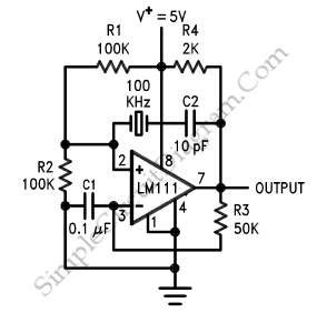
Create an oscillator circuit using an operational amplifier and a 7.68 MHz crystal. The design should be similar to the schematic provided below, but specifically tailored for a 7.68 MHz crystal. The available components include the crystal, various capacitors,...
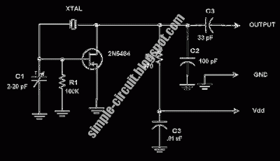
This circuit is a conventional Pierce-type oscillator that utilizes a JFET. It operates with fundamental mode crystals, offering decent performance and reliability when a low noise JFET is employed. The feedback is regulated by the capacitance of C1 from...
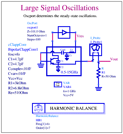
Oscillator cores (cClappCore, cHartleyCore, cModifiedClappCore, and cModifiedColpittsCore) are compatible with simulation and measurement setups outlined by the Generic Oscillator Example. These core oscillator circuits are configured for low resistance loads (50 ohms is used for these four oscillator cores,...
Warning: include(partials/cookie-banner.php): Failed to open stream: Permission denied in /var/www/html/nextgr/view-circuit.php on line 713
Warning: include(): Failed opening 'partials/cookie-banner.php' for inclusion (include_path='.:/usr/share/php') in /var/www/html/nextgr/view-circuit.php on line 713