
RF2132 linear power amplifier circuit diagram

The RF2132 linear power amplifier is designed to amplify RF signals with high efficiency and linearity. The architecture incorporates a preamplifier stage followed by a power amplifier stage, which collectively ensures that the input RF signal is effectively amplified. The direct coupling of the internal amplifier, coupled with a blocking capacitor, minimizes signal distortion and maintains the integrity of the RF signal throughout the amplification process.
The input impedance is standardized at 50 ohms, a common characteristic for RF applications, which facilitates compatibility with various RF sources and loads. The external matching network connected to pin 1 plays a critical role in fine-tuning the impedance to optimize performance based on specific application requirements.
Inductor L1 is pivotal for adjusting the output level at the center frequency, allowing for precise control over the amplifier's gain characteristics. Resistor R1 is strategically placed to enhance the linearity of the first-stage amplifier by adjusting its biasing conditions, which is essential for maintaining signal fidelity, especially when dealing with complex modulated signals.
Inductor L2 functions as a shunt inductor in the output stage, contributing to the overall stability and performance of the amplifier. The combination of capacitor C7 and the internal inductances at pins 14 and 15 is crucial for achieving resonance at the second harmonic frequency (2f0). This resonance effectively mitigates unwanted harmonics, thereby improving both the gain and efficiency of the amplifier, making it suitable for high-performance RF applications.
The output terminals (pins 10, 11, 14, and 15) are interconnected within the chip, ensuring a robust output stage capable of delivering the amplified RF signal to subsequent stages or loads. The power control pin (PC) at pin 8 allows for dynamic control of the amplifier's power state. By adjusting the voltage at this pin, the amplifier can be turned off at low control voltages (0.5V or lower), which is particularly useful for power management in battery-operated devices. The specified supply voltage (Vcc) of 4.8V and control voltage (Vpc) of 4.0V indicate the operational parameters under which the RF2132 is designed to function optimally. As shown in FIG constitute grounds RF2132 linear power amplifier circuit. Radio frequency (RF) signal from the input pin 3, via a preamplifier, after the last stage power ampli fier output is amplified by 10, 11 feet. 3 feet and internal amplifier is directly coupled, plus a blocking its coupling capacitor, the input impedance is 3 feet 50, but the exact value of the impedance between the internal level 1 pin external matching network decisions. L1 is between the center frequency of the output level adjustment inductors; R1 can be improved linearity, increasing the first-stage amplifier bias; L2 is the amplifier output stage shunt inductor; C7 with 14, 15 feet inside wiring inductances series resonance, the resonant frequency is 2f0, second harmonic output short circuit can effectively improve gain and efficiency.
Output terminals 10,11,14,15 feet inside the chip is connected. 8 feet to power control pin (PC), you can control the pin voltage to control the power supply. At room temperature, when the voltage is low (at 0.5V or lower), the amplifier power is turned off. Vcc 4.8V, Vpc 4.0V.
Related Circuits
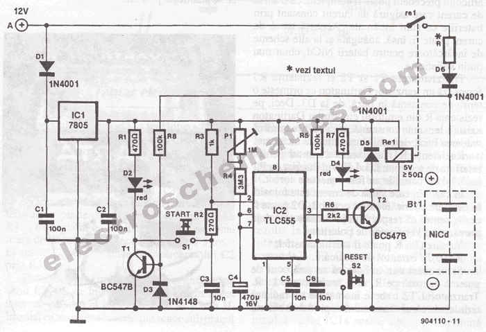
The portable battery charger has been designed to enable the charging of NiCd batteries outdoors using a 12 V vehicle battery. The portable battery charger is engineered to facilitate the charging of Nickel-Cadmium (NiCd) batteries in outdoor environments, leveraging the...
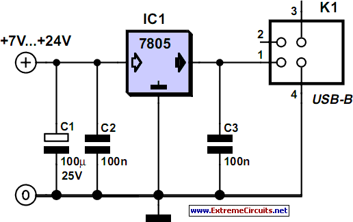
Although a matching charger is typically included in the package, some devices can only be charged via a USB port. This is not surprising for USB MP3 players, which need to dock with a PC for file transfers. However,...

The timer is activated by the zero-crossing voltage pulse. The time constant is defined by the combination of C5 and the resistors R14 and R15, which determines the conduction angle. The transistors T2 and T3 prevent the power switch...
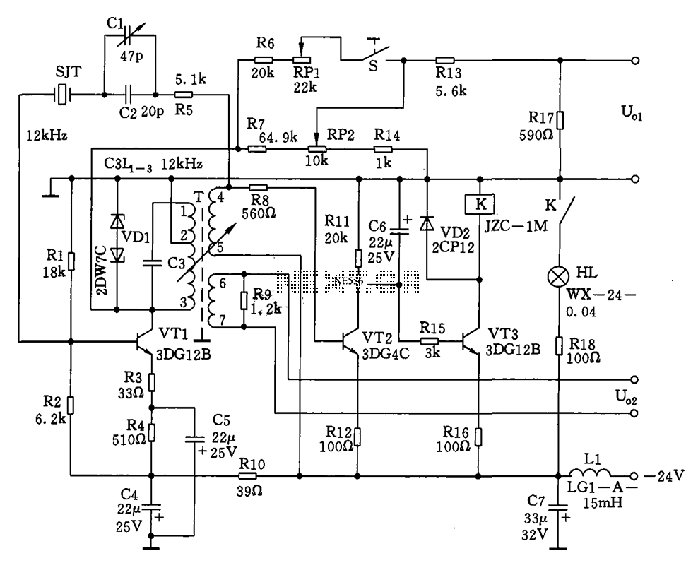
The circuit features a 12kHz intermediate frequency (IF) oscillator utilizing a quartz crystal for precision frequency generation. It includes components for output level adjustment, a level-up circuit, and an alarm circuit. The design employs a unique single-tuned variable feedback...
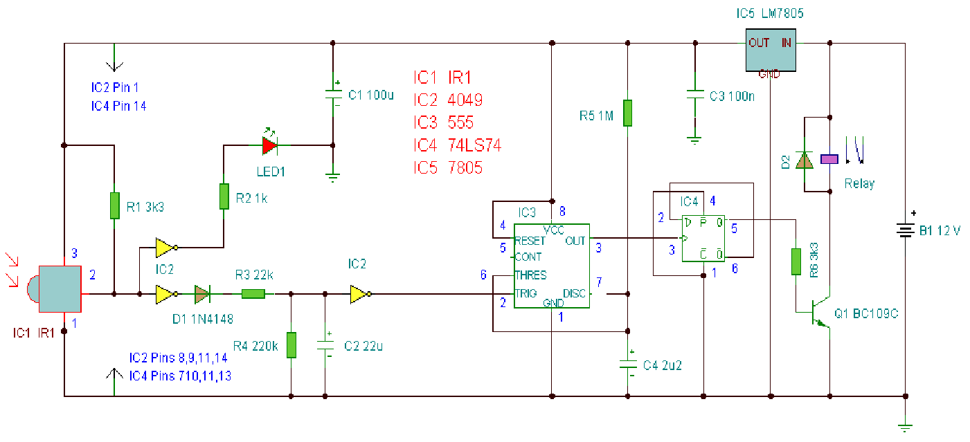
A computerized infrared remote project is a simple device designed for recording and playing back streams of infrared data, specifically the codes transmitted by remote controls. Software is provided for use in both DOS and Windows environments, along with...
This circuit can be programmed for a gain of 0, -1, -2, -4, or -8. This could also be accomplished with one input resistor and one feedback resistor per channel in the conventional manner, but this would require eight...