
Schmitt trigger with LM741 op-amp
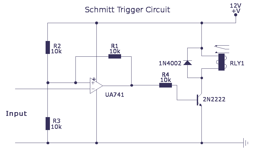
The Schmitt trigger circuit is a type of comparator that provides hysteresis, which is essential for eliminating noise in digital signals. The core component of this circuit is the operational amplifier (op-amp), specifically the LM741, which is configured to operate in a non-inverting mode. The input signal is fed into the non-inverting terminal of the op-amp, while the inverting terminal is connected to a voltage divider that sets the threshold levels for switching.
The output of the LM741 is then buffered by a transistor, which serves to amplify the current drive capability of the op-amp. This transistor can be an NPN type, such as the 2N3904, allowing it to control a relay or an LED based on the output state of the op-amp. When the op-amp output goes high, the transistor conducts, energizing the relay coil and closing the relay contacts to complete the circuit. If a red LED is used instead of a relay, it will illuminate when the op-amp output is high, providing a visual indication of the circuit's state.
The circuit can be powered by a dual supply voltage, typically ±15V, allowing the op-amp to swing its output close to the supply rails. However, it is important to note that real-world op-amps like the LM741 have output limitations, typically swinging to within 0.5V of the supply rails, which should be considered in the design.
For applications requiring improved performance, the LM741 can be substituted with a LF411 or other JFET input op-amps, which offer better slewing rates and bandwidth. This enhances the circuit's response time and accuracy, particularly in fast-switching applications.
The hysteresis effect is implemented by carefully selecting the feedback resistor values in the voltage divider connected to the inverting terminal. This creates two distinct threshold voltages: one for transitioning from low to high (Vth+) and another for transitioning from high to low (Vth-). The difference between these two thresholds is what provides the noise immunity, allowing the circuit to maintain stable operation in the presence of signal fluctuations.
Overall, the Schmitt trigger circuit is an effective solution for converting noisy signals into clean digital outputs, suitable for a variety of applications in electronics.The schmitt trigger circuit is built around a single LM741 op-amp, its output buffered by a transistor, which in turn energizes a relay. The relay may be replaced by a red LED if desired. The LM741 may be replaced by a LF411 or other JFET input op-amp with better slewing characteristics. An ideal op-amp would have infinite open loop gain, be able to swing its output to the full supply rails and have infinite slewing rate, bandwidth etc. In practise op-amps get swing their outputs to within 0.5V of the supply rail but have finite open loop
🔗 External reference
Related Circuits
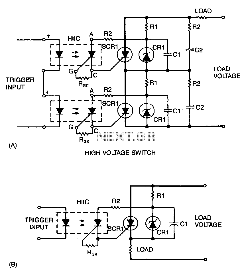
A snubber circuit consisting of R2 and C2 may be necessary, as R1 and C1 are designed for optimized triggering rather than for dV/dt protection. Fiber-optic pairs can be utilized with discrete SCRs to switch high voltages. A photonic...
The circuit is built around a single 4093 quad 2-input NAND Schmitt trigger. Two gates from that quad package (U1-a and U1-b) are configured as a set-reset flip-flop. The 4093 integrated circuit (IC) contains four independent 2-input NAND gates with...
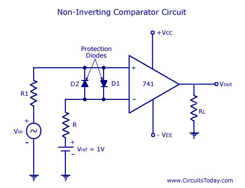
A working schematic diagram and design of the uA741 integrated circuit (IC) operational amplifier comparator circuit is provided, including the waveforms for both inverting and non-inverting comparators. The uA741 operational amplifier is a versatile component widely used in various applications,...
A conventional single junction transistor trigger circuit is limited to producing narrow pulses due to the rapid turn-off characteristics of the single-junction transistor. To address this limitation, a PNP transistor is added to the single-junction transistor trigger circuit, which...
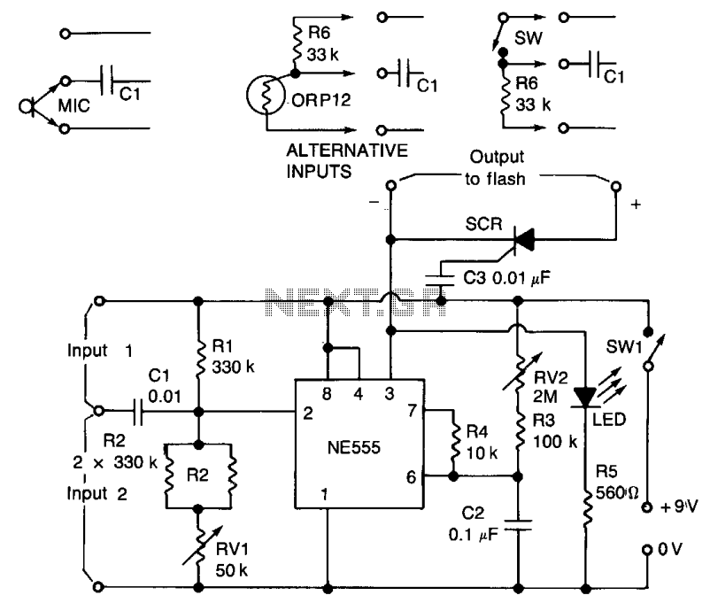
A negative pulse at the input is fed through capacitor C1 to the input pin (2) of the integrated circuit (IC). Pin 2 is maintained slightly above its triggering voltage of 1/3 Vcc by a voltage divider consisting of...
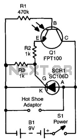
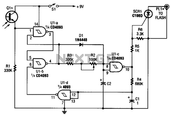
The SCR is connected across the trigger circuit of the flash gun. In its default state, the SCR remains off, allowing the flash gun to charge to its trigger voltage. A phototransistor, Q1, is utilized to monitor the light...