
Time Delay Flash Trigger Circuit Circuit
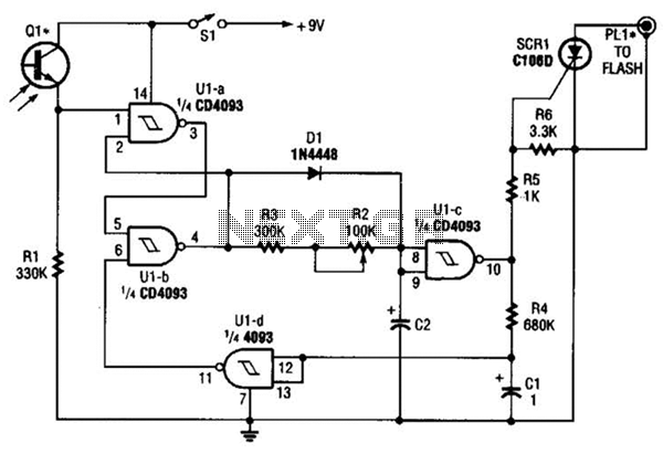
The 4093 integrated circuit (IC) contains four independent 2-input NAND gates with Schmitt trigger characteristics, which provide a high degree of noise immunity and are suitable for use in digital circuits requiring clean transitions. In this configuration, two of the NAND gates (U1-a and U1-b) are utilized to create a set-reset (SR) flip-flop.
The set-reset flip-flop operates by using the NAND gates to store a binary state. The output of U1-a is connected to one input of U1-b, while the output of U1-b is fed back to one input of U1-a, forming a feedback loop essential for maintaining the state of the flip-flop. The other inputs of both NAND gates are connected to the set (S) and reset (R) control signals. When the set input is activated (logic high), U1-a outputs a logic low, which in turn causes U1-b to output a logic high, thereby setting the flip-flop. Conversely, activating the reset input causes U1-b to output a logic low, which resets the output of U1-a to logic high.
This configuration allows for stable binary storage, where the outputs can remain in their respective states until the set or reset inputs are activated again. The Schmitt trigger action ensures that the transition between high and low states is clean, eliminating any unwanted oscillations or noise that could affect the reliability of the flip-flop operation. This circuit is commonly used in applications requiring memory storage, pulse generation, and state retention in digital systems. The circuit is built around a single 4093 quad 2-input NAND Schmitt trigger. Two gates from that quad package (Ul-a and Ul-b) are configured as a set-reset flip-flop. 🔗 External reference
Related Circuits
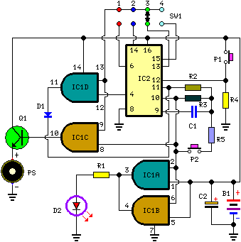
Pressing P1 resets IC2, which then begins oscillating at a frequency determined by R3 and C1. With the specified values, this frequency is approximately 4Hz. LED D2, controlled by IC1A and IC1B, flashes at the same oscillator frequency, indicating...
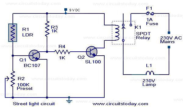
A street light that automatically switches ON when night falls and turns OFF when the sun rises. The circuit uses an LDR to sense the light. The automatic street light circuit functions by utilizing a Light Dependent Resistor (LDR) as...
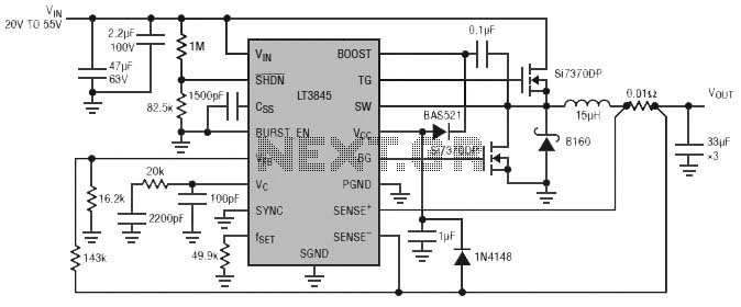
Burst Mode operation maintains high efficiency at light loads by reducing IC quiescent current to 120 µA. Light load efficiency is also improved with the reverse inductor current inhibit function, which supports discontinuous operation. Additional features include an adjustable...
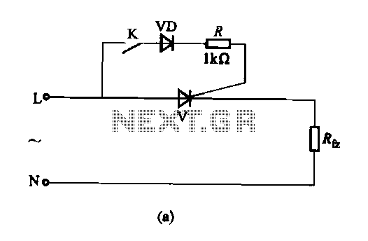
The thyristor AC switch circuit is not triggered, due to its simplicity, cost-effectiveness, and non-contact operation, making it widely utilized. The circuit is illustrated in Figure 16-43. It consists of single-phase thyristor switching circuits. Figure 16-43 (a) depicts a...
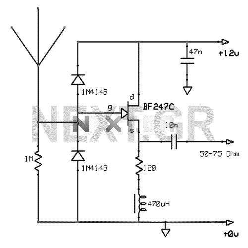
This active antenna schematic can be used to frequency range from 10 KHz to 100 MHz. The length of the Antenna can be between 0.5 to 1 meter long. The power consumption is 20-30mA. More: Use the shortest possible...
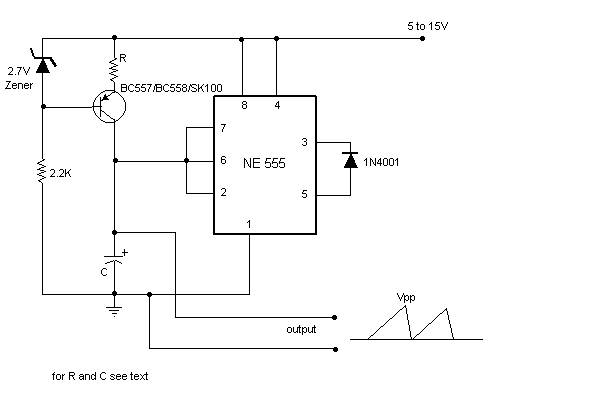
Sawtooth wave generators using opamp are very common. But the disadvantage is that it requires a bipolar power supply. A sawtooth wave generator can be built using a simple 555 timer IC and a transistor as shown in the...