
Summing-amplifier
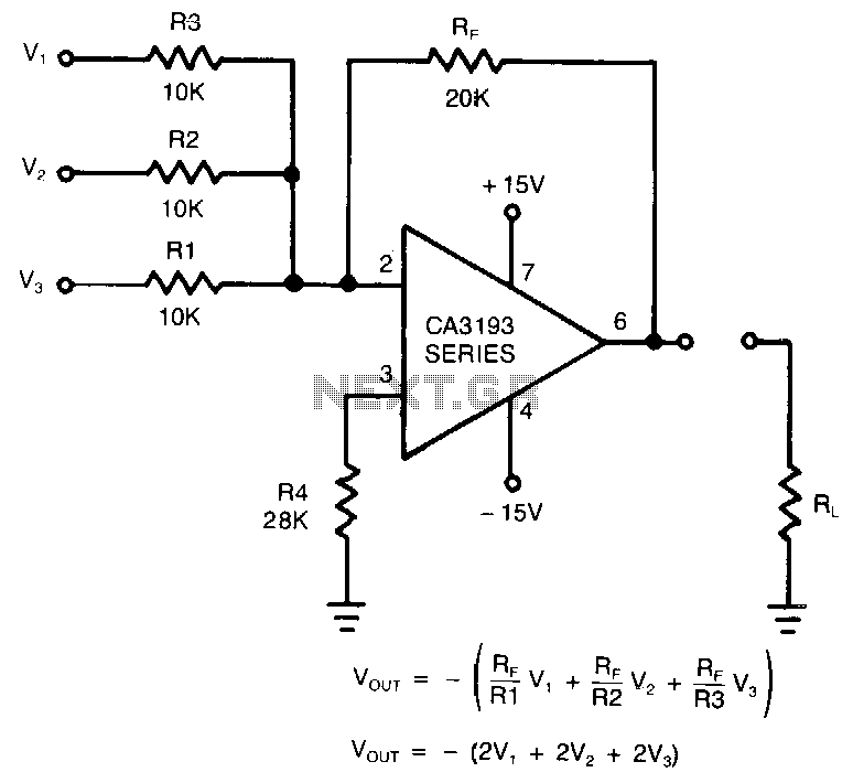
This circuit utilizes a CA3193 BiMOS operational amplifier. The input noise of the amplifier is influenced by the resistor network formed by Rp, Rl, R2, and R3. The gain provided by a single input channel is determined by the ratio of Rp to Rl. To achieve optimal noise performance, it is advisable to minimize the number of input channels used.
The CA3193 BiMOS operational amplifier is characterized by its low input noise and high-speed performance, making it suitable for various applications requiring precision signal amplification. The circuit design emphasizes the importance of resistor selection in managing input noise. The resistors Rp and Rl form a voltage divider that sets the gain for the selected input channel, while R2 and R3 may be used for feedback or additional gain control.
In this configuration, the input noise is a function of the parallel combination of Rl, R2, and R3, which can increase the overall noise level if not carefully managed. Therefore, to enhance the signal-to-noise ratio, it is recommended to keep the number of active input channels to a minimum. This approach not only reduces complexity but also helps maintain the integrity of the signal by limiting the contributions of extraneous noise sources.
For practical implementation, attention should be given to the layout of the circuit to minimize parasitic capacitances and inductances that may affect performance. Additionally, power supply decoupling capacitors should be employed near the op-amp to ensure stable operation and further reduce noise. Overall, the design should aim for a balance between gain, bandwidth, and noise performance to achieve the desired application objectives.This circuit uses a CA3193 BiMOS op amp. Because input noise of the amplifier is increased by Rp/ Rl//R2/ /R3, and the gain that a single input will amplify is the gain of only one of the input channels (Rp/ Rl), for good noise performance, use the smallest number of inputs. 🔗 External reference
Related Circuits
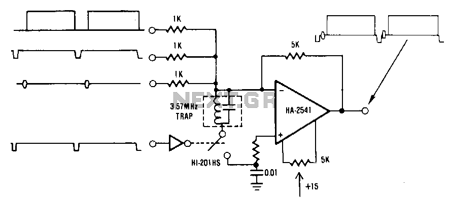
This circuit is a conventional summing amplifier configuration that incorporates a de-clamping circuit. The operation is straightforward; each component—synchronization, color burst, picture information, etc.—of the composite video signal is connected to its respective input terminal of the amplifier. These...