
SW RF Pre-Amplifier

The circuit design incorporates several key components to ensure optimal performance in amplifying weak radio signals while minimizing noise interference. The resistive attenuator at the input stage is crucial for protecting the receiver from strong signals that could lead to distortion or damage. The transformer, T1, serves as the main coupling device, with its carefully calculated turns ratio and inductance values tailored for the desired frequency range. The selection of wire gauge (22 SWG) is significant in balancing the resistance and inductance characteristics of the transformer.
The tuning capacitor configuration allows for fine adjustments across a critical frequency range. The use of a variable capacitor in conjunction with a fixed capacitor enables a flexible tuning mechanism. The calculation of effective capacitance when capacitors are placed in series is essential for achieving the desired resonance frequency, which directly influences the circuit's selectivity and sensitivity.
The 2N3819 FET, operating in common-source mode, is chosen for its high gain characteristics, which are vital for amplifying weak signals. The inclusion of a series base resistor (R1) is a common practice in RF design to mitigate high-frequency response issues, ensuring that the circuit remains stable across its operational bandwidth. The addition of a choke in the drain circuit helps to maintain the integrity of the amplified signal while managing the load presented to the FET.
The output stage, utilizing the BC108C transistor in an emitter follower configuration, effectively buffers the high output impedance of the FET, allowing for better interfacing with subsequent stages or output loads. The overall current consumption of approximately 3 mA from a 9 Volt source indicates a low-power design, suitable for portable applications.
To enhance performance, the circuit should be housed in a shielded enclosure to reduce susceptibility to external noise and interference, which is a common issue in RF applications. The successful operation of the circuit on a breadboard indicates its robustness and effectiveness in boosting weak radio signals.The problem with amplifying weak radio signals is that you also amplify the noise. What you can receive depends on how much background noise is present, whether it be man made interference or static. In this design the RF signal is first met by a resistive attenuator, this is necessary as strong signals could otherwise overload your receiver.
The transformer T1 is would on a 1 inch diameter ferrite loop. The primary (antenna side) is 2 turns of 22 swg wire. The secondary is 4 turns of 22 swg wire. The 4 turns are spaced to occupy roughly half the coils circumference. The approximate inductance of the secondary is 20uH. To cover 5 to 20 Mhz a capacitor tuning from around 3pF to 200pF is required. A standard capacitor of 400 or 500pF (full mesh) can be used by including a series capacitor, C2 in the above Capacitors. Capacitors in series behave the same as resistors in parallel. The smallest capacitance is just less than the smallest capacitor in series and highest value also less than the highest capacitance.
With a 220pF capacitor for C2 and a 500pF variable capacitor (that tunes down to 5pF) the effective capacitance tunes 143pF to about 4. 8pF. This is roughly correct and not critical as the gain of the FET will amplify frequencies outside the tuned circuit range.
The 2N3819 FET operates in common source. The series base resistor R1 is included to even out the response, the internal gate source impedance is thus increased by R1 at higher frequencies. The drain circuit includes a 2. 5mH choke. A 4. 7mH can also be used. As the Q factor of these coils are high, a series resistor R3 is introduced to flatten the response. The frequency response is shown below calculated at 10% increments of VC1: The output impedance from the FET is high, so is buffered by the BC108C in emitter follower mode.
Current drain is around 3mA from a 9 Volt battery. As with any RF circuit, the circuit is sensitive to noise and interference. A metal or aluminum box would be a good choice for this project. However, on my trusty breadboard, this circuit preformed well, and weak signals were boosted well. 🔗 External reference
Related Circuits
A section of the operational amplifier's output signal is rectified using 1N4148 diodes, followed by filtering, and is then directed to the gate of the FET input shunting circuit. As the output voltage increases, additional input shunting occurs, which...
Circuit description of a VHF pre-amplifier using a grounded base configuration. The VHF pre-amplifier circuit utilizing a grounded base configuration is designed to amplify very high-frequency signals while maintaining a low noise figure and high input impedance. This configuration is...
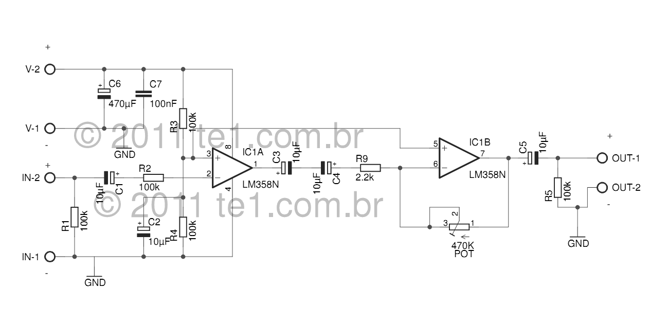
The LM358 series consists of two independent, high-gain, internally frequency-compensated operational amplifiers designed specifically to operate from a single power supply over a wide range of voltages. Operation from split power supplies is also possible, and the low power...
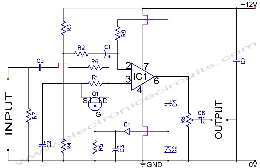
Many designers assert that NFB loop controlled amplifiers are inferior because they degrade the sound. However, it's worth considering what these individuals believe they are actually listening to. The reality is that most vinyl waveforms and CD pits, as part...

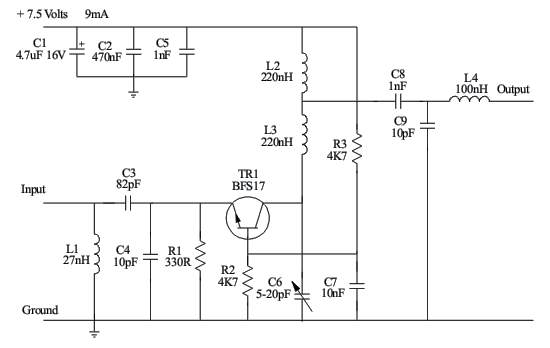
The following circuit illustrates a VHF pre-amplifier circuit diagram. This circuit utilizes the BFS17 transistor. Features: designed for VHF applications. The VHF pre-amplifier circuit is essential for enhancing weak radio frequency signals in the VHF (Very High Frequency) range, typically...
This is a microphone preamplifier designed for compatibility with a SoundBlaster AWE 64 sound card. It is also suitable for any compatible tag or PC audio input that provides a 5 Volt supply through a 2.2kΩ current-limiting resistor located...