
Synchronized Mains Voltage Power Control
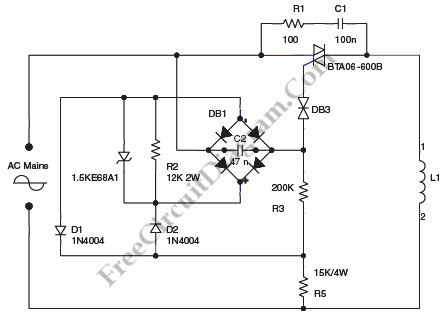
The step-down circuit is designed to reduce the input voltage level to a more manageable value for the inductive load (L1), which is critical in applications where high voltage levels could damage sensitive components. The circuit employs a combination of passive components to achieve this voltage regulation.
The turn-on delay of approximately 7 ms is a crucial feature, allowing the circuit to stabilize before the inductive load is energized. This delay is determined by the time constant formed by capacitor C2 and resistor R3, calculated as τ = R3 × C2. This time constant ensures that the capacitor charges to a sufficient voltage before the load is activated, thereby preventing inrush currents that could lead to circuit instability or component failure.
The discharge mechanism for capacitor C2 is facilitated by the diode bridge comprising diodes D1 and D2. This arrangement allows C2 to discharge rapidly at each zero voltage crossing of the line input, effectively resetting the voltage across the capacitor. Resistor R2 plays a role in limiting the discharge current, ensuring that the diodes operate within their specified current ratings while also influencing the speed of the discharge process.
The circuit's design ensures that the voltage across the load is reset with each new half line cycle, maintaining the turn-on delay consistently across cycles. This feature is particularly beneficial in applications requiring precise timing and voltage control, such as in motor control circuits or lighting systems where inductive loads are prevalent. Overall, this step-down circuit effectively balances the need for voltage reduction with the operational requirements of inductive load management.A step-down circuit used to approximately divide by two the rms voltage between the line input and the inductive load (L1) is shown on circuit diagram below. A turn-on delay of approximately 7 ms is provided by C2 and R3. We can discharge C2 at each line zero voltage using diode bridge, with diodes D1 and D2 and R2 resistor.
The voltage charge wil l be reset at each new half line cycle, and the turn-on delay will be maintained the same. 🔗 External reference
Related Circuits
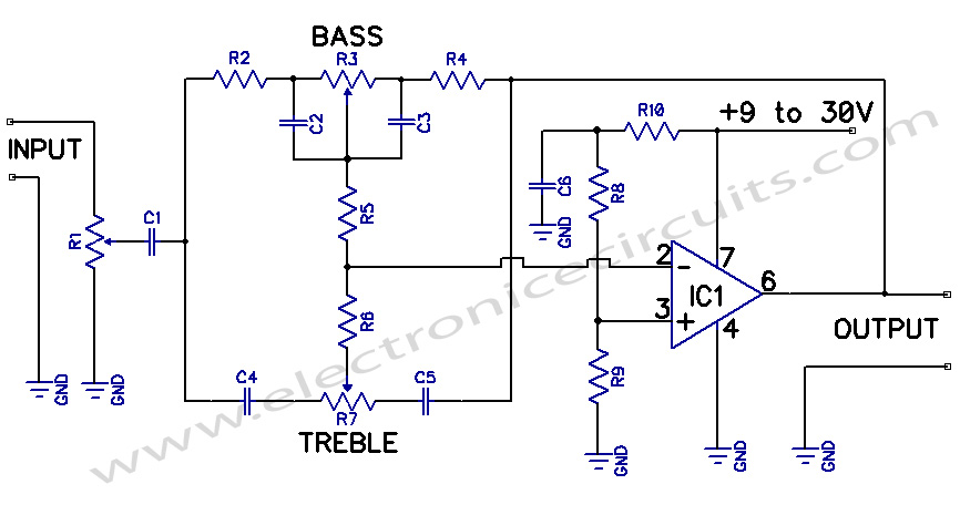
A preamplifier circuit featuring independent Bass and Treble tone controls is illustrated in this schematic. This circuit design utilizes operational amplifiers (op-amps) to achieve independent control over the bass and treble frequencies, allowing for enhanced audio customization. The preamplifier stage...
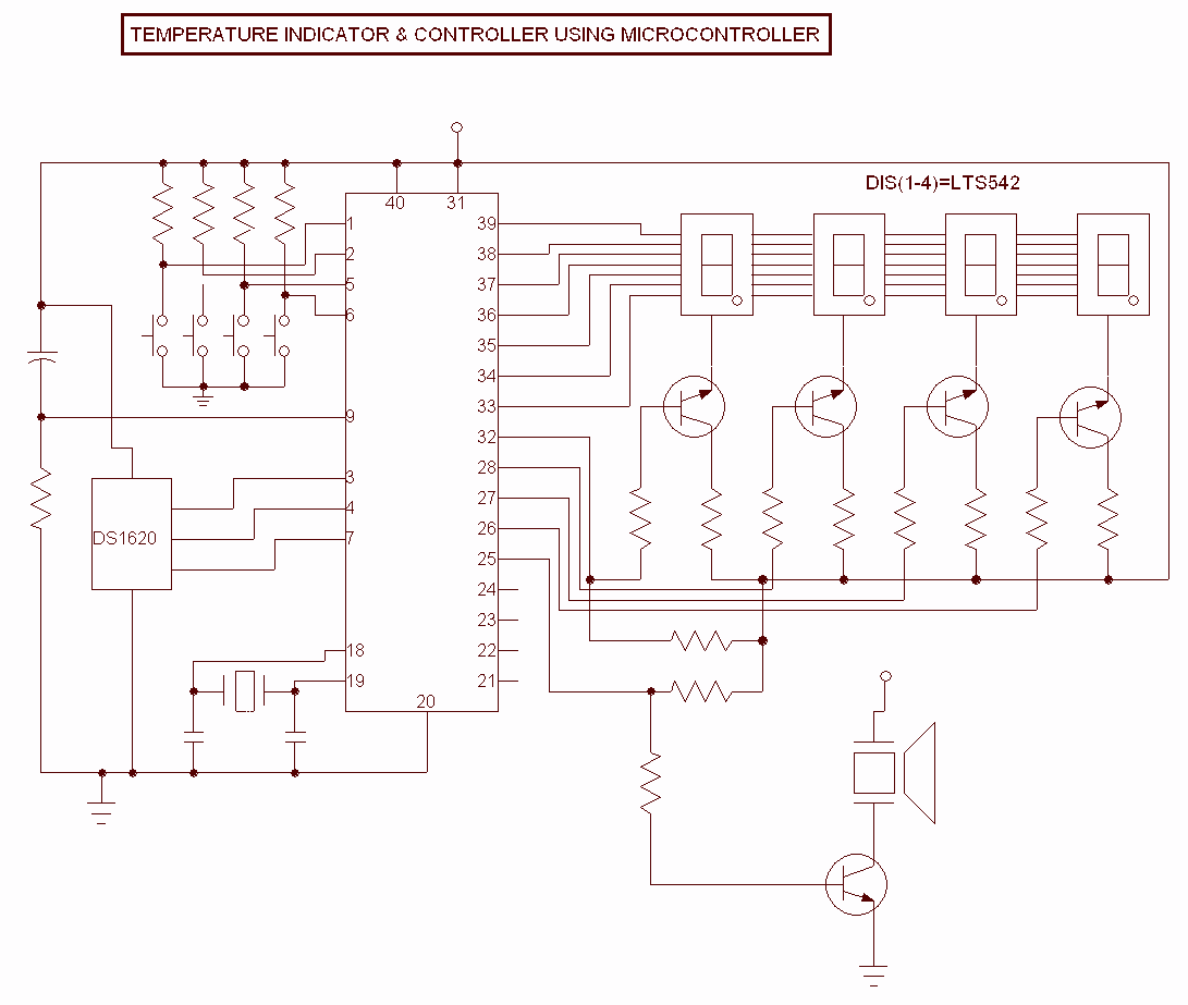
This Project is used to indicate the temperature and it is also used as controller. The system will get the temperature from the IC and it will display the temperature over the seven segment display and this temperature was...
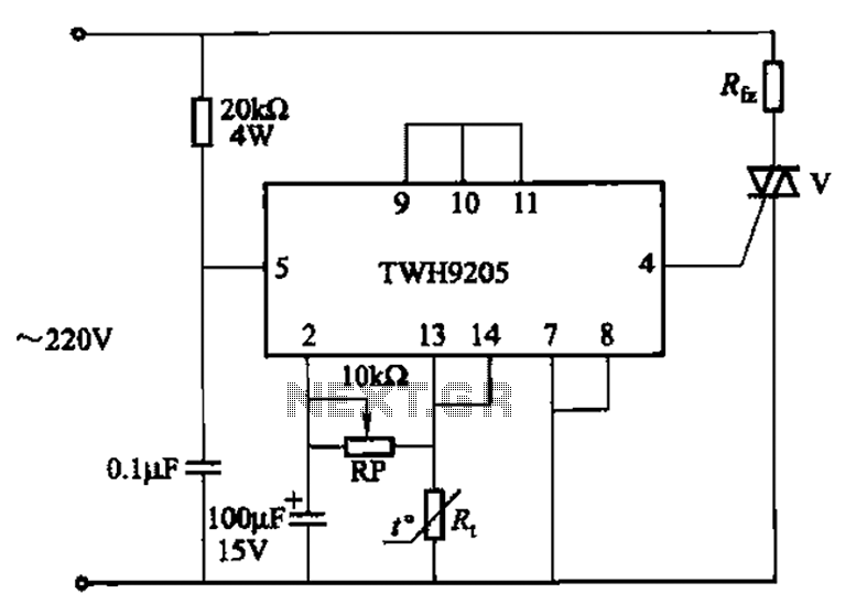
This circuit is used for temperature control in various heating equipment such as water heaters, microwave ovens, air conditioners, refrigerators, fans, and automatic fire extinguishing devices. It includes a negative temperature coefficient (NTC) thermistor as the temperature sensing element...
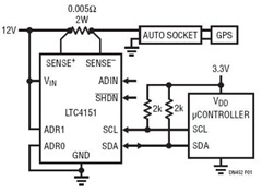
This power monitoring device accurately measures voltage and current on a positive supply rail ranging from 7V to 80V through a straightforward I2C interface, as specified in the datasheet. It is particularly suitable for automotive applications that require power...
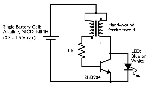
This circuit is commonly referred to as a Joule Thief, and it has been frequently encountered in various electronics videos on YouTube. The Joule Thief is a simple, low-cost circuit designed to extract energy from a single-cell battery, particularly when...
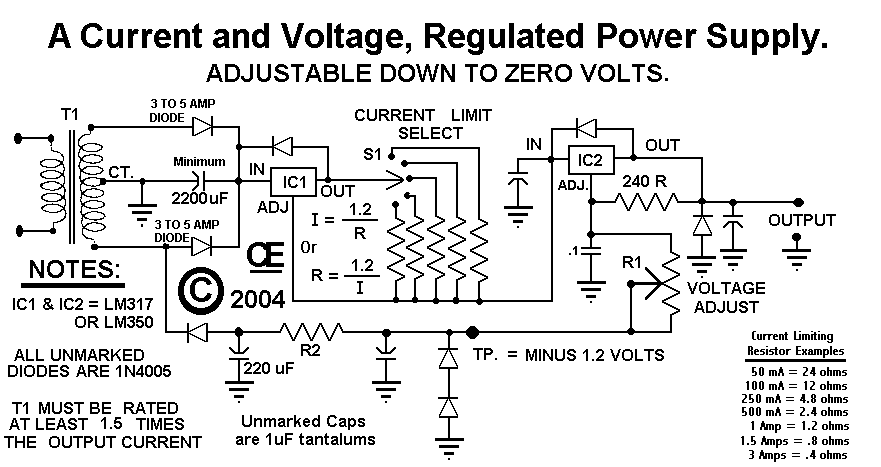
This circuit employs a rotary switch to select various current ranges, as using a potentiometer is not practical for lower resistance and high current ranges. However, a potentiometer can be utilized for lower current ranges, with the lowest switch...