
TDA1514A application circuit
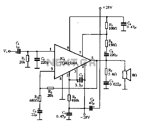
The TDA1514A integrated circuit is designed for audio amplification applications, typically used in car radios and other high-fidelity audio devices. The feedback circuit formed by resistors R2 and R3 is crucial for setting the gain of the amplifier; adjusting these resistors changes the feedback ratio, thereby modifying the overall gain of the circuit to suit specific requirements.
The bootstrap circuit, consisting of capacitor C5 and resistor R5, plays a vital role in improving the amplifier's dynamic range. This configuration allows for better handling of transient signals, ensuring that the amplifier can respond quickly to changes in the audio signal without distortion. The noise suppression mechanism, involving capacitor Q, is essential for maintaining audio clarity by minimizing unwanted noise that could interfere with the output signal.
Capacitor C is strategically placed to ensure that any voltage fluctuations do not affect the performance of the amplifier. By maintaining a stable voltage across C, the circuit ensures that the power supplied to pin V3 remains consistent, which is critical for the operation of the silent-circuit switch. This switch is responsible for muting the output during power-up or power-down conditions, thereby preventing audible pops or clicks that could be detrimental to speakers.
Capacitor C4's role in the circuit is equally significant. As it charges, it influences the voltage at pin 3, which is pivotal in controlling the silent switch. When the voltage reaches a predetermined level, the circuit automatically disengages the mute function, allowing the amplifier to resume normal operation without manual intervention. This feature enhances user experience by providing seamless transitions between muted and active states.
Resistor R, which is part of the protection circuitry, is designed to limit the quiescent current to a safe level, ensuring that the amplifier operates efficiently without drawing excessive power during idle states. This design consideration is crucial for battery-operated applications, where power conservation is a priority. Overall, the circuit design for the TDA1514A integrates various components to ensure optimal performance, reliability, and user satisfaction in audio amplification applications.For its typical application circuit o R2, R3 is a feedback circuit to adjust their ratio, adjustable circuit loop gain o To increase the dynamic range of the circuit, the C5 and R5, R bootstrap circuit. TDA1514A boot noise suppression is achieved by capacitor Q. In the instantaneous power, the voltage across the capacitor C can not be mutated, so the power of a V 3 without loss to the feet, forcing silent-circuit switch circuit is activated to power the noise is suppressed. With the charging capacitor C4, when it was raised to the voltage across a V value, 3-pin voltage falls to zero, forcing and 3 feet in contact Silent switch is automatically released and the amplifier power amplifier function properly realized.
R is the resistance of the protected zones and set up, and under normal circumstances, 2 feet microamps quiescent current.
Related Circuits
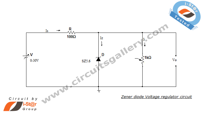
A Zener diode regulator is a fundamental electronic circuit valuable for hobbyists. This circuit provides a regulated output voltage, suitable for biasing other circuit components. The Zener diode operates in the reverse breakdown region, maintaining a nearly constant voltage...
A magnetic switch is a circuit designed to respond to surrounding magnetic fields detected by the sensor. This series of magnetic switches employs limit switch sensors that include an additional metal plate capable of responding to a magnet. The...
Using a transistor will not yield accurate results, and the adjustment process can become quite tedious. The circuit is technically correct; if the tripping point can be adjusted properly, it may function as intended. Vinod states that he created...
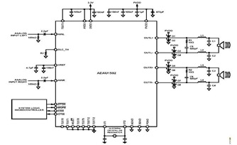
This is a typical stereo application circuit schematic of the ADAU1592, a 2-channel, bridge-tied load (BTL) switching audio power amplifier. The ADAU1592 can be utilized in flat panel televisions, PC audio systems, and mini-component applications. The ADAU1592 is designed to...

If the reader arrived here via Google, they may have encountered other circuits for high-power LED driving that include many components such as inductors, operational amplifiers, various regulator ICs, transistor feedback networks, and microcontrollers. While those circuits tend to...
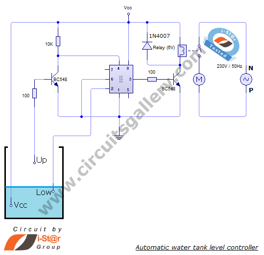
The automatic water level controller circuit is a straightforward engineering project that can automatically switch a domestic water pump on and off based on the water level in a tank. This motor driver circuit can be implemented at home...