
The bilateral band modem circuit composed of NE561B
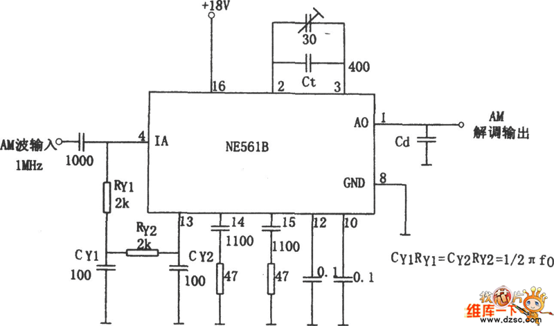
The bilateral band modem circuit featuring the NE561B is designed to facilitate efficient modulation and demodulation of signals. The NE561B is a versatile integrated circuit widely used in communication systems for its ability to perform analog multiplication and phase detection.
In this specific configuration, the input modulating signal at a frequency of 1 MHz is critical for the operation of the circuit. The amplitude modulation (AM) signal, when fed into the multiplier, is essential for generating the desired output modulation. The phase detection circuit, which includes resistive and capacitive elements (Rv1, CY1, Y2, and CY2), plays a crucial role in maintaining synchronization between the modulated signal and the voltage-controlled oscillator (VCO) frequency of the phase-locked loop (PLL).
The phase detection circuit ensures that any phase discrepancies between the input signal and the VCO output are corrected, thereby stabilizing the frequency output at f0. The use of capacitors and resistors in this configuration helps filter and shape the signals, ensuring that only the desired frequency components are processed.
Overall, this circuit design exemplifies a robust approach to signal modulation, leveraging the NE561B's capabilities to achieve effective communication in various electronic applications. The careful selection of components and their arrangement within the circuit is vital for optimal performance and reliability in real-world scenarios.In the figure is the bilateral band modem circuit composed of NE561B. The loading frequency of the input modulating signal is f0=1MHz. When the AM modulation signal is added on the input terminal of the multiplier, it is also added on the phase detection circuit by Rv1, CY1, Y2 and CY2, and it sets the VCO frequency of PLL at f0.. 🔗 External reference
Related Circuits
To extend the measurement range of an available ADC (analog to digital converter), autoranging can be utilized. If implemented on multiplexed input, this... Autoranging is a technique employed in electronic measurement systems to automatically adjust the range of an analog-to-digital...

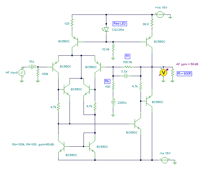
This amplifier was designed to utilize the otherwise unused TO3 power transistors that many hobbyists possess. With proper construction, the module can achieve high-quality performance and is rated for 300 watts into a 4-ohm load, depending on the power...

The Zener diode functions as an avalanche rectifier in reverse bias mode, connected to the input circuit of a wideband RF amplifier. The noise is amplified and subsequently applied to the cascade wideband amplifier, utilizing transistors Q2 and Q3. The...
This circuit utilizes two operational amplifiers (op-amps) to create a unique sound effect. The first op-amp, CA741, is configured as a standard astable multivibrator, generating timing pulses controlled by components C1, R2, and variable resistor VR1. The output from...
For bikers or scooter riders, it is common to forget to cancel flashing indicators after making a turn, especially without an audible reminder. Continuously checking indicator lamps is impractical, as attention should remain focused on the road. The circuit...
This circuit was submitted by Graham Maynard from Newtownabbey, Northern Ireland. It has an exceptionally fast high-frequency response, as demonstrated by applying a 100kHz square wave to the input. All graphs were produced using Tina Pro. The circuit in question...
Warning: include(partials/cookie-banner.php): Failed to open stream: Permission denied in /var/www/html/nextgr/view-circuit.php on line 713
Warning: include(): Failed opening 'partials/cookie-banner.php' for inclusion (include_path='.:/usr/share/php') in /var/www/html/nextgr/view-circuit.php on line 713