
Noise generator circuit

The circuit incorporates a Zener diode configured to operate in reverse bias, allowing it to maintain a stable voltage across its terminals. This characteristic is critical in RF applications, where maintaining signal integrity is essential. The Zener diode effectively clamps voltage spikes and provides voltage regulation, ensuring that the input signal to the wideband RF amplifier remains within acceptable limits.
In this specific configuration, the Zener diode is positioned at the input of the wideband RF amplifier to mitigate any unwanted noise that may interfere with the amplification process. The subsequent stages of the amplifier are comprised of transistors Q2 and Q3, which are configured in a cascade arrangement. This configuration allows for enhanced gain and improved bandwidth, making it suitable for a wide range of RF applications.
The noise picked up by the input circuit is amplified by the first stage, which is critical for improving the signal-to-noise ratio (SNR). The amplified signal is then fed into the next stage, where Q2 and Q3 further boost the signal strength. This cascading effect is vital for achieving the desired amplification levels, ensuring that the output signal is robust enough for further processing or transmission.
Overall, the integration of the Zener diode within the input circuit of the wideband RF amplifier plays a crucial role in maintaining signal integrity and enhancing the overall performance of the amplifier system.The zener diode is an avalanche rectifier in the reverse bias mode connected toiihe input circuit ofa wideband rf amplifier The noise is amplified and applied to the cascade wideband amplifier, transistors Q2 and Q3. 🔗 External reference
Related Circuits
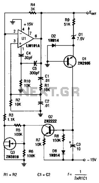
For variable-frequency operation, Rl and R2 can be replaced by a dual potentiometer. In electronic circuits that require variable-frequency operation, the use of a dual potentiometer as a replacement for resistors Rl and R2 can provide enhanced functionality and flexibility....

The liquid level automatic controller circuit consists of a power circuit, a control instruction level detection circuit, and a starter control circuit. The power circuit is formed by a power transformer, a rectifier bridge, and a filter capacitor. The...
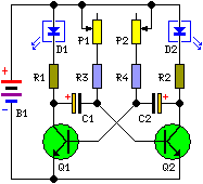
This circuit diagram illustrates a setup for two flashing LEDs designed for various applications, including model construction and recreational uses. It features adjustable flashing speeds controlled by two potentiometers. The circuit comprises a combination of active and passive components....
This light-dependent sensor utilizes light-dependent resistors (LDRs) to detect the presence or absence of light. The alarm remains inactive as long as the light source illuminating the LDRs is constant. However, if the light is interrupted, the alarm is activated. The...
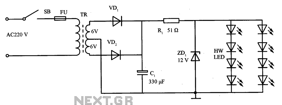
The schematic for the LED lighting circuit in a refrigerator consists of eight high-brightness white LED lights. These LEDs are housed in a transparent white plastic tube, which is the same height as the refrigerator cabinet. The circuit receives...
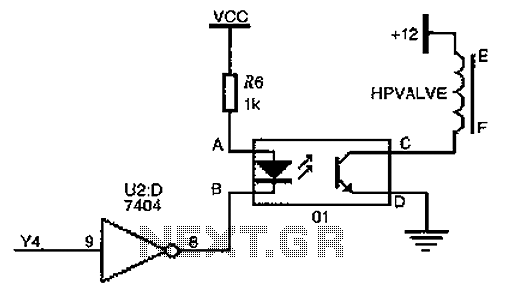
The driver circuit for the high-pressure natural gas shut-off valve utilizes solid-state relays. In dual-fuel mode operation, the fuel switching mechanism is controlled by a logic section that activates Y4 to a high state via U2 (7404 inverters). This...