
The single-phase sine wave frequency conversion stabilized voltage supply is designed and made
The circuit described employs a robust design approach to ensure stable output voltage and current under varying input conditions. The use of SPWM allows for efficient control of the output waveform, enhancing the performance of the voltage supply. The single-phase half-controlled rectifier configuration is advantageous for applications requiring adjustable output, while the integration of an uncontrolled rectifier simplifies the overall design by reducing component complexity. The RC over-voltage protection circuit effectively manages transient conditions, safeguarding sensitive components from voltage spikes.
The unijunction transistor flip-flop configuration is a cost-effective solution for generating control signals, ensuring reliable operation of the thyristors. The inverter design utilizing BJTs allows for efficient switching and minimal power loss, making it suitable for various applications. The feedback mechanism provided by diodes D1 and D2 enhances the energy efficiency of the system by recycling energy back into the circuit.
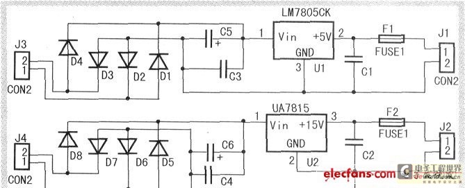
Furthermore, the inclusion of a 555 timer-based multivibrator and JK flip-flops ensures precise frequency control, which is crucial for applications requiring specific timing characteristics. The voltage regulator circuit effectively stabilizes the supply voltages necessary for the operation of the power amplifiers, contributing to the overall reliability of the system. The frequency measurement module serves as an essential tool for monitoring circuit performance, allowing for real-time adjustments and ensuring compliance with design specifications. This comprehensive approach to circuit design highlights the importance of component selection, configuration, and protection in achieving a reliable and efficient voltage supply system.When the input voltage is 198- 242V, the mean value of the load current is 0. 5- 1A, the mean value of the output voltage should keep in 15V, the error is smaller than 5% : 1 When the input voltage is 198- 242V, the mean value of the load current is 0. 5- 1A, the mean value of the output voltage should keep in 15V, the error is smaller than 1%; 2 Design and make and measure, reveal the circuit of the output voltage of stabilized voltage supply, electric current, frequency and power of this frequency conversion, the error in emasurement is smaller than 5%. 1 Can use, produce SPWM Puls e-width modulation of sine wave Corrugate special purpose chip; 2 The output power can be calculated through the measured value of the electric current, voltage.
Single-phase rectifying circuit: The following picture of choosing the rectifying circuit of single-phase half control is shown. This circuit control is flexible, the adjustable within the specific limits of the magnitude of output voltage, so become the selected scheme.
But we find while finishing this part of a circuit. The flip flop of this circuit has certain difficulty. Under not making the situation that the rigid index stipulates to the rectifier while designing the index, we can well adopt the single-phase uncontrolled rectifying circuit, thus reduce the design of the flip flop of two triode thyristors. Originally design RC over voltage killer circuit R9, C5 adopted to connect in parallel in the second order of the voltage transformer Component side, In order to absorb the released energy of unshakable in one`s determination magnetic field of the voltage transformer.
And change and store it for electric field energy of the capacitor, series resistance for consume some energy and inhibit the intersection of RC and vibration that loop might produce from in energy transduction. R10, C6 are regarded as the capacitance-resistance protective circuit of straight flow side. The flip flop of the rectifying circuit is chosen by the unijunction transistor BT33 Q3 The constituent flip flop, the following picture, shows, though phase shift range and power are not high, but low cost, satisfiable designing requirement, so become the selected scheme.
The trigger impulse that VD1, VD2 output, as the triggering signal of VT1 and VT2 triode thyristor. Change and touch off the angular magnitude by regulating the potentiometer RP0, thus change the magnitude of the direct-current volts of the output. Reverse the stabilizator and choose the right side circuit of the following picture of inverter circuit with central tapped transformer to be shown.
Drive two power BJT V1, V2 alternatively, Couple and for load to add to the square wave alternating current voltage by the voltage transformer. Two diodes D1, D2 Function last energy too feedback channel. The advantage of this circuit is that controlling circuit is simple, the component protects technology ripely.
It is because its price is cheap to reverse the on-off element and choose BJT tube of the power, it is flexible to control. The single-phase frequency conversion control device chooses by 555 U1 Make up multivibrator and JK JPl The flip-flop constituent facelift and left side circuit of the following picture of amplifying circuit of V4, V5 constituent final-stage are shown.
The frequency accuracy of this circuit control is high, flexible and convenient, can finish the designing requirement index. By 555 U1 And JK JP1 The flip-flop is the active device, so the following picture of still needing to produce 5V and 15V direct-flow voltage regulator circuit in addition is shown, bias direct-current volts source as it, 15V stabilized voltage supply is still two power amplifier tubes V3, V4 Offer the bias voltage.
According to the designing requirement, the measurement of the frequency adopts the display module of single frequency. Need to make a LED frequency counter, is used for revealing t 🔗 External reference
Related Circuits
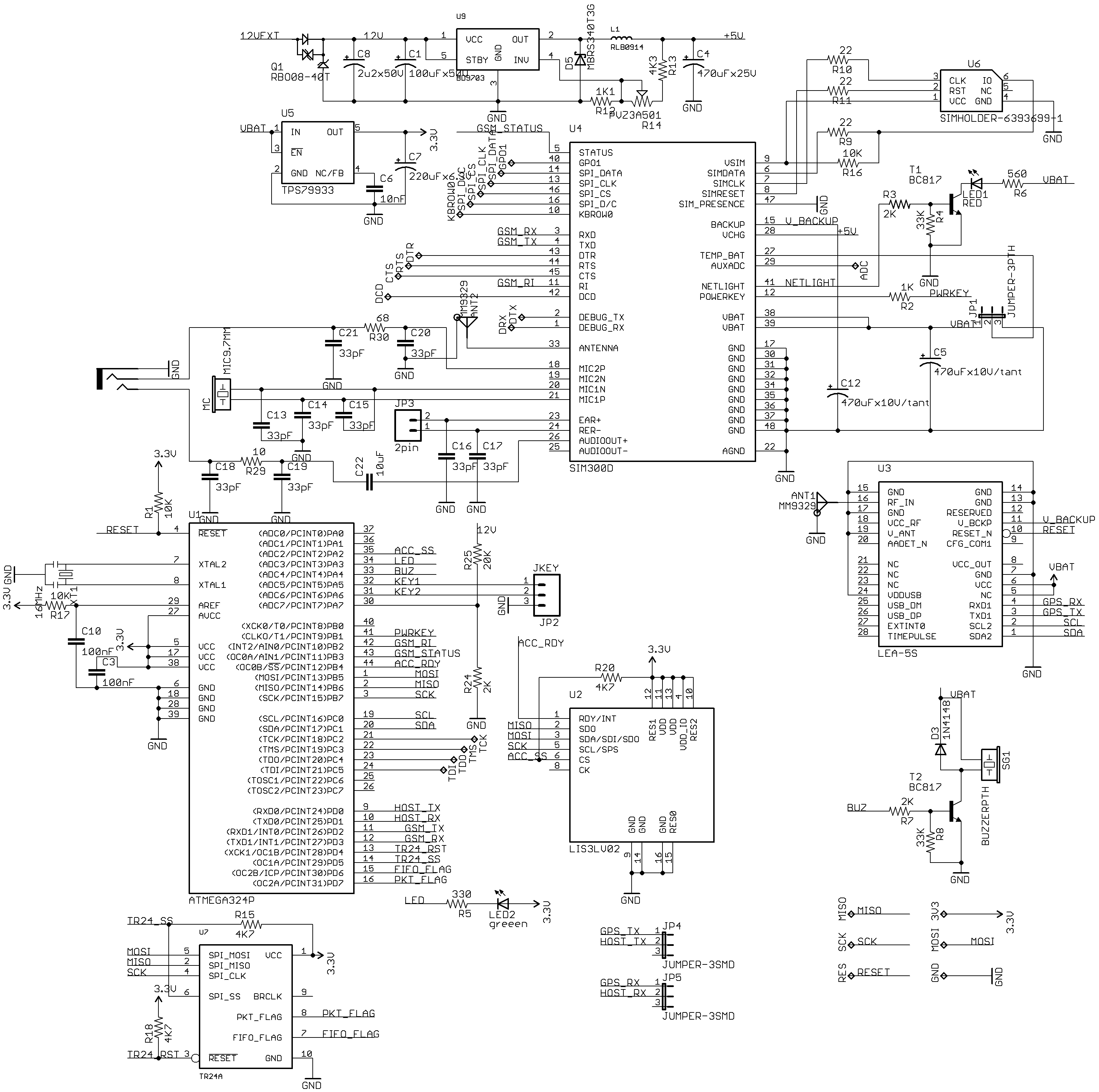
New uTracker on GE865 with a compact design. This updated version of the tracker features the SIM300DZ and EB-230/LEA-5S modules. It includes an OBD-II (ISO) sensor, an accelerometer, and an RFID reader. Additionally, a TR24 2.4GHz module is incorporated,...
The outputs in this circuit are independently variable and can be loaded unsymmetrically. The output voltage remains constant, regardless of load and changes. By varying potentiometers R2 or R6, the output voltages can be conveniently set. Outputs can be...
In a binary phase shift keying (BPSK) modulation scheme, the phase of a carrier signal is altered according to digital pulse signals. The BPSK modulator functions as a phase modulator, where the transmitted signal is a sinusoid with a...
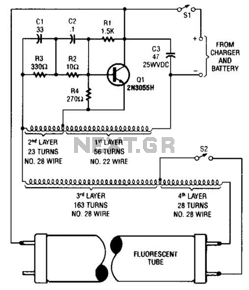
A 2N3055 oscillator (Q1) drives a homemade transformer, wound on a Vk ferrite rod. S2 is used as a filament switch and can be eliminated if desired. A 20-W fluorescent tube is recommended. The supply voltage is 12 V. The...
The design is based on the TubeHobby and serves as the power supply used in their NC2. This kit was constructed as an initial project involving nixie tubes, and a review of this excellent kit can be found in...
A frequency meter is commonly used in speed sensors, tachometers, and for measuring recurring signals. This frequency-to-voltage converter (FVC) can be utilized to convert frequency into a digital or analog tachometer output. The circuit comprises three main blocks. The...
Warning: include(partials/cookie-banner.php): Failed to open stream: Permission denied in /var/www/html/nextgr/view-circuit.php on line 713
Warning: include(): Failed opening 'partials/cookie-banner.php' for inclusion (include_path='.:/usr/share/php') in /var/www/html/nextgr/view-circuit.php on line 713