
thermostat design

The circuit design involves the integration of a Programmable Logic Device (PLD) to manage the control of multiple seven-segment displays by processing temperature data from an Analog to Digital Converter (ADC). The ADC will output 8 signals, which will serve as inputs to the PLD. The PLD is tasked with decoding these inputs and generating 14 output signals to illuminate the appropriate segments of the seven-segment displays, thus providing a visual representation of the temperature readings.
The ADC will output a limited range of values, specifically 15 discrete intervals corresponding to specific temperature measurements. This selective use of the ADC's output is designed to simplify the display logic within the PLD. The VHDL code provided outlines the architecture of the PLD, indicating the input and output ports and the process that governs the display updates based on the temperature input. Each case in the process corresponds to a specific temperature value, with the corresponding seven-segment display configuration defined for each temperature range.
To ensure accurate temperature readings, a thermistor is employed, which requires balancing through a Wheatstone bridge configuration using 20-ohm resistors. This configuration is critical for achieving a zero-volt output at room temperature. The bridge's output will be connected to an operational amplifier (Op-Amp) configured as a differential amplifier. The differential setup allows for the amplification of the voltage difference between the two sides of the bridge. It is anticipated that as the temperature increases, the voltage output from the bridge will decrease, necessitating a gain to ensure the signal remains within a measurable range.
The selected Op-Amp, the LM341, is chosen for its ability to provide a closed-loop gain of 10, which is essential for amplifying the small voltage changes expected from the thermistor. The Op-Amp's output will then feed into the ADC0804, which has been configured similarly to previous projects, allowing for straightforward integration into the existing circuit. Proper grounding and reference voltage levels are crucial for the ADC's operation, ensuring accurate digital representation of the analog signal derived from the thermistor.
In summary, this circuit design combines a PLD, thermistor, operational amplifier, and ADC to create a robust system for temperature measurement and display. The careful selection of components and configuration details aims to ensure reliable performance and accurate temperature representation on the seven-segment displays.We are planning to use a Programmable Logic Device to control our seven-segment displays. This will be accomplished by using the 8 outputs from the Analog to Digital converter as the inputs to the PLD, and by having the PLD generate 14 outputs to drive the 7 segments of each display. In our design, only 15 of the possible 256 intervals output from the Analog to Digital converter will be used, each corresponding to a specific temperature in degrees. We plan to configure our PLD basically at first, and then refine the program once the rest of the circuit has been implemented.
LIBRARY IEEE; USE IEEE. std_logic_1164. all; use IEEE. std_logic_unsigned. all; ENTITY jeff IS PORT(temperature : in std_logic_vector (7 downto 0); clk : in std_logic; display : out std_logic_vector (13 downto 0); END jeff; ARCHITECTURE interior of jeff is BEGIN PROCESS (clk) BEGIN if (rising_edge(clk) then case temperature is when "00000000" => display <= "10110111001111"; -23 when "00000101" => display <= "10110111011011"; -22 when "00001010" => display <= "10110110000110"; -21 when "00001111" => display <= "10110110111111"; -20 when "00010100" => display <= "00001101100111"; -19 when "00011001" => display <= "00001101111111"; -18 when "00011110" => display <= "00001100000111"; -17 when "00100100" => display <= "00001101111100"; -16 when "00101000" => display <= "00001101101101"; -15 when "00101101" => display <= "00001101100110"; -14 when "00110011" => display <= "00001101001111"; -13 when "00110111" => display <= "00001101011011"; -12 when "00111100" => display <= "00001100000110"; -11 when "01000001" => display <= "00001100111111"; -10 when "01000110" => display <= "01111111100111"; -09 when others => display <= "11110011111001"; -EE end case; end if; end PROCESS; END interior; In order to `Balance` our Thermistor, so that 0 volts were being output when the thermistor was at room temperature, we needed to construct a bridging circuit. The thermistor we are using has a listed base resistance of 20 ohms, for this reason we constructed the bridge using 20 ohm resistors.
As can be seen in the diagram, we are planning to connect the bridge to our Operational Amplifier in a differential configuration (ie, connect two input voltages and take the difference). The inputs to the Op-Amp will be the two sides of the bridge, which side corresponds to positive and which to negative will be determined after the bridging circuit has been constructed.
It should also be mentioned that in our configuration, as the temperature of the thermistor decreases, we are expecting the output voltage from the bridging circuit to increase, whereas when the temperature of the thermistor increases, the voltage should then decrease. We are also planning to have quite a substantial gain, since our thermistor will more than likely only change by a very small margin, probably around 0.
5 mV for its entire range. The final section of our circuit is the Operational Amplifier ( LM341 ), which was connected to our Analog to Digital converter ( ADC0804 ). First, the Op-Amp. As was mentioned in the previous section, the output of the bridging circuit was quite low, thus we needed an Op-Amp with a built in gain, for this application we chose a closed loop gain of 10.
Since we were dealing with two inputs (the positive and negative sides of the bridge), we needed to construct a differential amplifier which would amplify the difference of the two inputs. The circuit we implemented was constructed according to the following picture: Now, for the Analog to Digital Converter.
This was a fairly simple portion of the project, since the converter was wired in the same manner as in the `Digital to Analog and Analog to Digital` lab. The wiring was identical to the following diagram: All digital grounds in the diagram (pins 10, 19, and 4) were considered to be analog grounds.
The `Vref/2` on pin 9 was accomplished with the aid of a 2 1/2 volt 🔗 External reference
Related Circuits
A diode, such as the IN4148, has a typical temperature coefficient of -2 mV/°C at a 1 mA diode current. Transistors Q1 and Q2 form a constant current source. Diode D1 serves as the temperature sensor. Integrated circuits ICl-a...
The FAN7710 Ballast Control IC for Compact Fluorescent Lamps, developed using Fairchild's unique high-voltage process and system-in-package (SiP) concept, enables the design of a simple and low-cost fluorescent lamp driver electronic project. The FAN7710 ballast control manages internal high-voltage...

This circuit features high stability and precision, providing a direct current source that can be preset for various electronic devices. The numerical control direct current source designed here effectively reduces output errors caused by component wear, temperature drift, and...
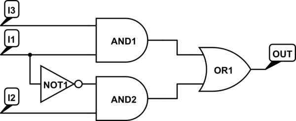
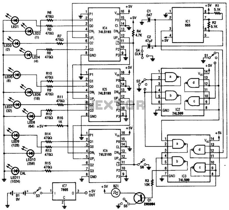
There are integrated circuits that contain AND, OR, and NOT gates. The inquiry revolves around the existence of a single chip that encompasses all the required logic gates. If such a chip does not exist, specific alternatives should be...
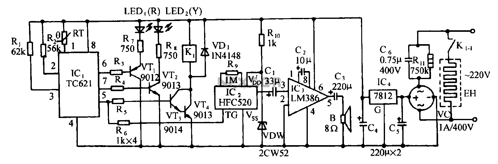
Eggs hatch chicks at temperature requirements within the range of 36 to 39 degrees Celsius. The temperature sensor integrated circuits utilize the TC621 temperature control circuit, which has fewer external components, is low cost, and offers high reliability. Users...
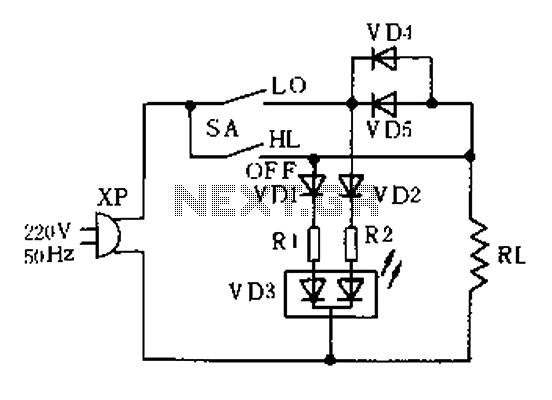
The thermostat electric circuit operates as depicted in the figure. It has three settings: off, low power (Lo), and high power (Peru HL). When the DIP switch SA is set to the Lo position, 220V AC is directed through...