
TTL Three - State Logic Probe PCB
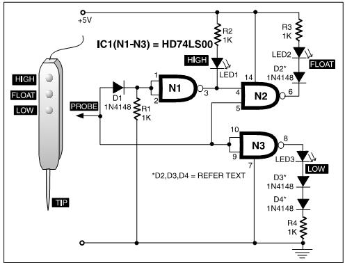
The TTL logic probe circuit using the HD74LS00 quad-NAND IC is designed to provide clear visual feedback regarding the logic levels present in a digital circuit. This probe operates in three distinct states: high, low, and high impedance (three-state operation), which allows the user to determine the state of a digital signal without significantly affecting the circuit under test.
The configuration of Gate N1 is critical for indicating a high logic state. When the input to Gate N1 is at logic 1, the output transitions to logic 0, which in turn activates LED1. This visual cue is essential for technicians and engineers as it indicates that the point being probed is at a high state, essential for diagnosing digital circuits.
Conversely, Gate N3 is configured to illuminate LED3 when its output goes high, indicating that the point being tested is at a logic 0 level. This dual-indicator system allows for quick and efficient troubleshooting, as the user can easily ascertain whether a signal is high or low at a glance.
In the implementation of this circuit, the choice of the HD74LS00 IC is particularly advantageous due to its low power consumption and fast switching times, which are beneficial in high-speed digital applications. The use of diodes D2, D3, and D4 further enhances the circuit's flexibility, allowing for compatibility with various other TTL families, ensuring that the logic probe can be adapted for use with different integrated circuits as necessary.
Overall, this TTL logic probe circuit is a powerful tool for digital circuit analysis, providing essential functionality in a compact form factor, making it invaluable for engineers and technicians working in electronics.A TTL logic probe is an indispensable tool for digital circuit troubleshooting. Various methods can be used to design a logic probe. The most common designs employ opamps, logic (OR, NOT, XOR) gates, and transistors. The circuit presented here uses NAND logic gates of Hitachi HD series IC HD74LS00, which is a quad-NAND IC. Special technique has be en employed to obtain three-state operation using just a single IC. In the circuit Gate N1 is wired such that when the output of gate N1 is at logic 0` (i. e. when its input is at logic 1`), LED1 will glow, to indicate high state of the point being probed. Gate N3 is wired to light LED3 when the output of gate N3 is high or when the point being tested is at logic 0` level. At power-on, the output of If any other type of IC (e. g. 74HCT00 or 74LS00) is used, diodes D2-D3-D4 should be added or deleted as necessary; for example, when using HD74LS00, one diode D2 is required.
🔗 External reference
Related Circuits
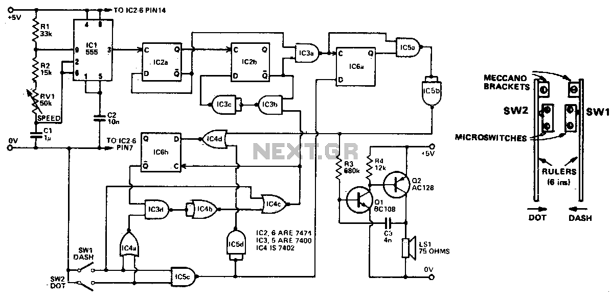
Automatically generated dits and dahs are produced over a speed range of 11 to 39 wpm. The upper limit can be raised by decreasing R2. SW1 and SW2 can be a "homebrew" paddle operated key. The described circuit is designed...
The circuit is functioning well, and there are no signs of withdrawal or autonomic instability. The focus is on the "DT" data column in the WSPR GUI, which tracks time differences. Recently, large and seemingly random timing errors were...
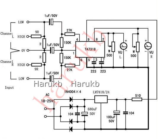
VU Meter Driver PCB Completed Board Stereo for Two VU Meters Audio Amplifier. VU Meter Driver PCB Completed TA7318P Board Stereo for Two VU Meters Features: Specifications: Power voltage: AC 20V to AC 26V (not more than 26V) size:...
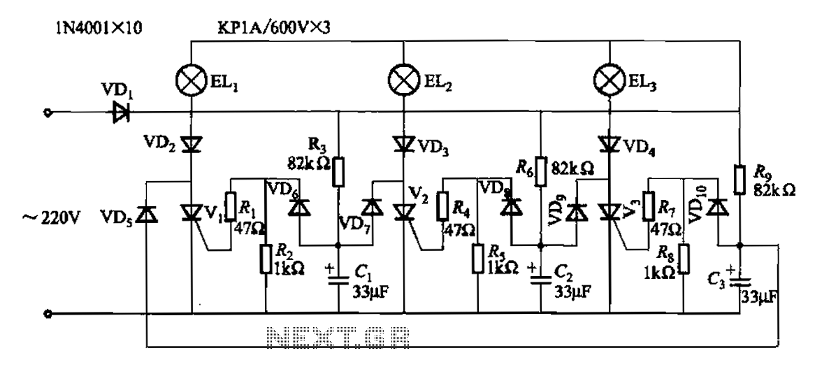
The circuit operates with a 220V mains supply through a diode (VDi) configured as a half-wave rectifier. Capacitors C1 to C3 are charged, and due to the lack of full synchronization in the charging process, a pilot thyristor is...
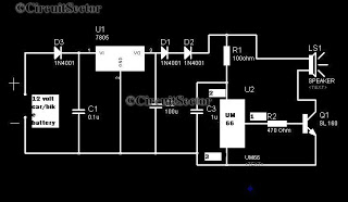
A simple musical horn circuit designed for use in cars or motorcycles can be connected to the 12V battery of any vehicle. This circuit is commonly utilized as a reverse musical horn. It employs the low-cost musical integrated circuit...
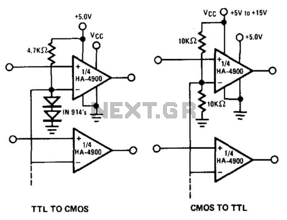
The HA-4900 series comparators can be utilized as versatile logic interface devices, as illustrated in these circuits. Negative logic devices can also be interfaced with appropriate supply connections. If separate supplies are employed for V- and VLogic-, these logic-level...
Warning: include(partials/cookie-banner.php): Failed to open stream: Permission denied in /var/www/html/nextgr/view-circuit.php on line 713
Warning: include(): Failed opening 'partials/cookie-banner.php' for inclusion (include_path='.:/usr/share/php') in /var/www/html/nextgr/view-circuit.php on line 713