
Tunable single comparator oscillator
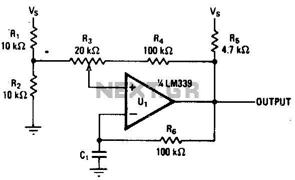
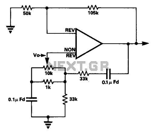
The comparator circuit operates by comparing two input voltages and producing a digital output based on which input is higher. The inclusion of hysteresis in the circuit design introduces a feedback mechanism that prevents rapid toggling of the output when the input voltage fluctuates around the threshold value. This stability is crucial in applications where noise might otherwise cause erratic behavior.
The hysteresis can be adjusted by modifying the feedback resistor values, which alters the reference voltage for the comparator. This adjustment enables the output frequency to be varied smoothly across the specified range. The time constant, determined by the product of resistor R6 and capacitor C1, plays a pivotal role in defining the charging and discharging behavior of the circuit. A larger time constant results in slower transitions, while a smaller time constant allows for faster changes.
In practical applications, this circuit can be employed in frequency modulation systems, pulse width modulation, and other signal processing tasks where precise control over frequency output is required. The design must ensure that the components selected can handle the desired frequency range and provide sufficient stability and response time for the intended application. Proper selection of R6 and C1 values is essential to achieve the desired hysteresis and time constant characteristics, ensuring optimal performance of the comparator circuit.Varying the amount of this comparator circuit"s hysteresis makes it possible to vary output frequencies in the 740-Hz to 2-kHz range smoothly The amount of hysteresis together with time constant R6C1 determines how much time it takes for CI to charge or discharge to the new threshold after the output voltage switches. 🔗 External reference
Related Circuits
The circuit is designed exclusively for fundamental crystals, as it lacks mode suppression components. The oscillator transistor Q104 remains in a cutoff state for most of the time, activating only briefly during the peak of the crystal current waveform....
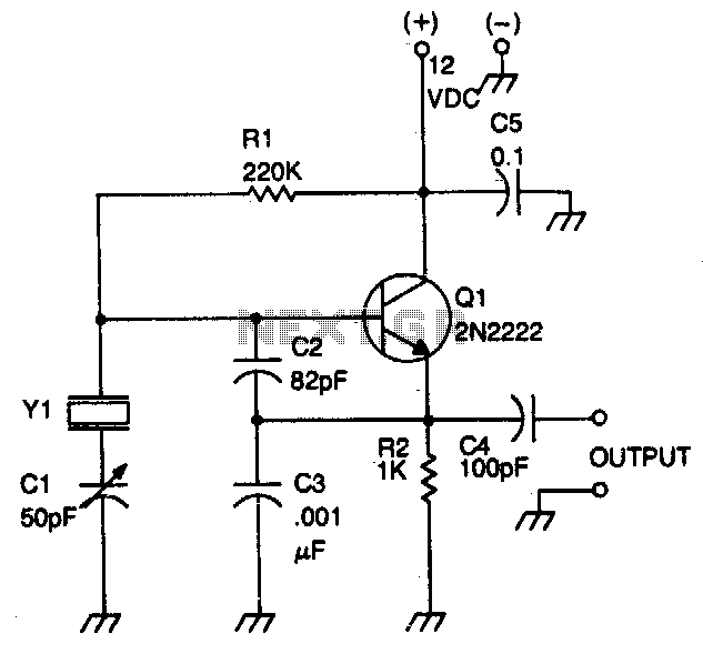
This circuit operates with fundamental-mode crystals in the frequency range of 1 MHz to 20 MHz. Feedback is regulated by the capacitor voltage divider formed by capacitors C2 and C3. The RF voltage across the emitter resistor supplies the...
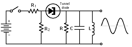
The excess small forward current flow in a tunnel or Esaki diode is a manifestation of quantum mechanical tunneling. Tunnel diodes, also known as Esaki diodes, are semiconductor devices that exploit the quantum mechanical phenomenon of tunneling to achieve their...
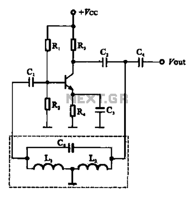
A three-point oscillator, also known as a Hartley oscillator, is similar to the Colpitts oscillator; however, its feedback circuit consists of two series inductors and a capacitor. The three-point oscillator is a type of electronic oscillator that generates sine waves....

A simple yet effective circuit to generate a POTS-compatible ringing voltage can be constructed using National Semiconductor's LM4871 audio amplifier IC along with a dozen passive components. This circuit produces a sine-wave output of 1 W at approximately 70...
In the circuit, the frequency trimming component is configured such that the voltage across it is in quadrature with the voltage V0 from the bridge. This arrangement allows for adjustments to be made with minimal changes to the attenuation...
Warning: include(partials/cookie-banner.php): Failed to open stream: Permission denied in /var/www/html/nextgr/view-circuit.php on line 713
Warning: include(): Failed opening 'partials/cookie-banner.php' for inclusion (include_path='.:/usr/share/php') in /var/www/html/nextgr/view-circuit.php on line 713