
Crystal Oscillators

The circuit operates primarily as a low-noise oscillator, optimized for use with fundamental mode crystals. The absence of mode suppression components indicates that this design is focused on achieving maximum stability and performance at the fundamental frequency of operation. The oscillator transistor Q104 is strategically cut off for the majority of its cycle, allowing for reduced power consumption and minimizing unwanted noise during inactive periods. The regulation of the DC collector current through Q103 ensures that the oscillator maintains consistent performance, with R116 serving as a critical component in adjusting the crystal current to desired levels.
The filtering stage, implemented by the combination of R101, R102, C101, and E102, is essential for attenuating high-frequency noise from the power supply, thereby enhancing the overall signal integrity of the oscillator. The use of four LM329 buried zener diodes provides a stable reference voltage, which is crucial for maintaining the oscillator's performance across varying conditions. The buffering action of Q105, along with the compensation provided by Q106, ensures that the voltage levels remain stable, minimizing the impact of any fluctuations that could lead to phase noise.
Furthermore, the design incorporates a common base buffer configuration with Q102, which effectively isolates the oscillator from load variations while maintaining low flicker phase noise. The careful selection of components and their configurations within the circuit reflects a thorough understanding of noise reduction techniques, ensuring that the oscillator operates with minimal interference. This design is particularly suitable for applications requiring high precision and stability, such as in communication systems or frequency synthesis. Overall, the circuit exemplifies a well-engineered approach to achieving low-noise oscillation while ensuring robust performance characteristics.The circuit is only suitable for fundamental crystals as there are no mode suppression components. The oscillator transistor Q104 is cutoff most of the time except for a short period at the peak of the crystal current waveform. Q103 regulates the dc collector current of the oscillator transistor Q103. The dc collector current of Q104 and hence the crystal current is set by the value of R116. Darlington transistor Q101 buffers the output of the filter (R101, R102, C101, E102) which low pass filters the power supply noise above 0. 16Hz. The oscillator supply voltage is produced by low pass filtering the average output of 4x LM329 buried zener references (Z101-Z103).
Q105 buffers the low pass filter output and Q106 compensates for the base emitter voltage drop of Q105. The collector base voltage of the oscillator transistor Q104 is relatively high to reduce its collector base capacitance and its voltage sensitivity.
This, together with the low dc gain from Q104 base to collector, keeps Q104`s contribution to the oscillator flicker phase noise low. Common base buffer transistor Q102 has a low dc gain (0. 5x) from base to collector, its emitter current is set by LED101, and R108 so that the buffer flicker phase noise is low.
The low noise oscillator power supply ensures that the modulation of oscillator transistor collector base capacitance by power supply noise and hence the power supply induced oscillator phase noise is low. 🔗 External reference
Related Circuits
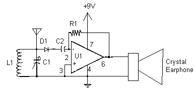
Here is a simple radio that is easy to build and inexpensive. In fact, you probably have all the parts you need in your junk box. You'll be surprised at the great reception with this little set. More: The...
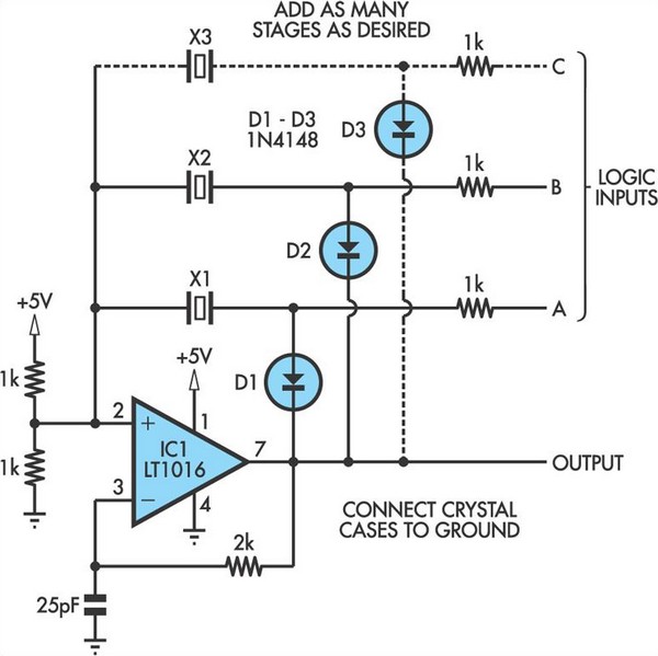
This oscillator circuit allows crystals to be electronically switched by logic commands. To understand the circuit, it is helpful to initially disregard all crystals and consider all diodes as shorts while their associated 1kΩ resistors are treated as open....

Another frequency-determining device is the crystal. The crystal may be used with a tank circuit, or it may function independently. Crystals exhibit a characteristic known as the piezoelectric effect, which is the property of a crystal that allows mechanical...
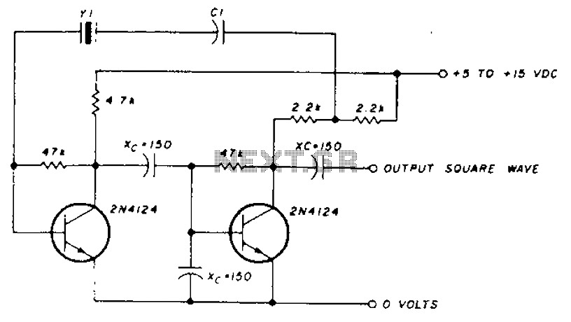
A transistor in series with capacitor C1 can be utilized to adjust the oscillator output frequency. The frequency may vary with changes in capacitance ranging from 20 pF to 0.01 µF, or as determined by the tuning capacitor. The...
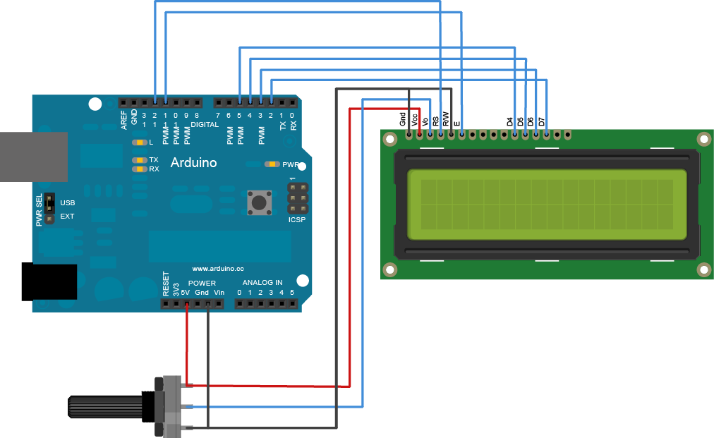
The Liquid Crystal Library enables control of LCD displays compatible with the Hitachi HD44780 driver. Many such displays are available, typically identifiable by their 16-pin interface. It is advisable to solder a pin header strip to the 14 (or...

The Motorola company's MC14440 CMOS integrated circuit is designed for timing and displaying calendar functions. It utilizes a 32.768 kHz NT cutting type quartz crystal along with fine-tune capacitance to generate time-based signals. The display circuit operates on a...