
Unsteady direct coupling circuit diagram
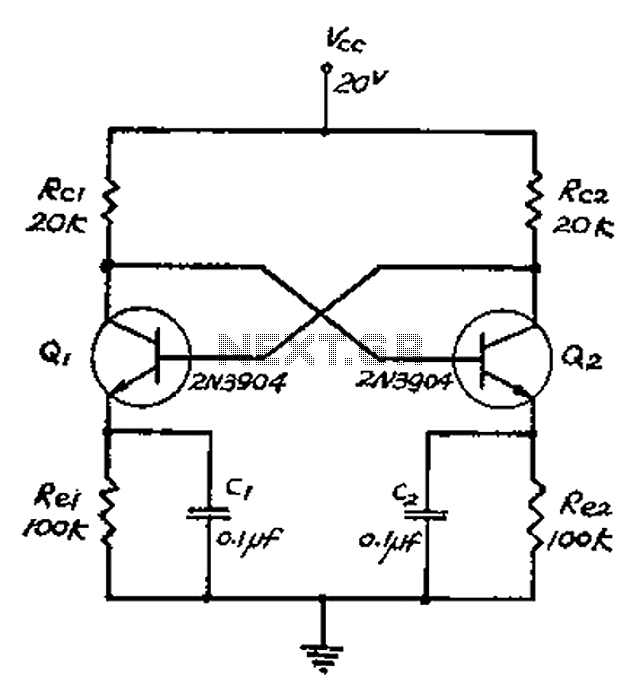
In this circuit configuration, the direct coupling of the collector and base-emitter bias establishes a feedback mechanism that enhances the performance of the transistors. The triangular wave generated by the emitter serves as a modulation signal, which is essential for applications requiring signal processing or waveform generation.
The operation of the circuit is characterized by its ability to switch between two distinct states. These states correspond to the charging and discharging phases of the capacitive elements in the circuit. During the charging phase, the circuit allows current to flow into the capacitors, storing energy. Conversely, during the discharging phase, the stored energy is released, facilitating the conversion of electrical energy.
The design of this circuit is particularly useful in applications such as signal modulation, where the triangular wave can be used to create varying voltage levels that can be transmitted or processed further. Additionally, the ability to switch states efficiently enables the circuit to conserve power, as the transistors are not continuously active, reducing thermal dissipation and enhancing overall reliability.
The implementation of such a circuit requires careful consideration of component values, including the resistors and capacitors, to ensure the desired frequency and amplitude of the triangular wave are achieved. Moreover, the selection of transistors with appropriate characteristics is crucial to optimize performance and efficiency in the intended application. Overall, the described circuit offers a robust solution for applications requiring effective signal modulation and energy conversion. Both collector and base-emitter bias transistor is coupled directly to each other. Each transmitter circuit capacity control conversion function. The emitter generates a triang ular wave. Two transistors are not always kept awake state. In contrast, the circuit has two fixed state, between these states charge and discharge capacity can be achieved conversion.
Related Circuits
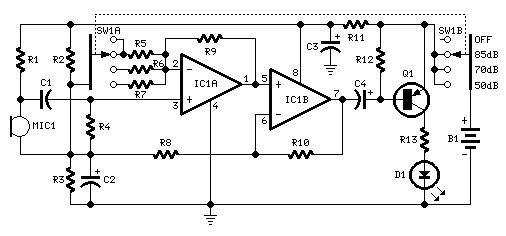
This circuit is designed to signal the exceeding of a fixed threshold in room noise through a flashing LED. Three fixed levels are selectable: 50, 70, and 85 dB. Two operational amplifiers provide the necessary gain for sounds captured...
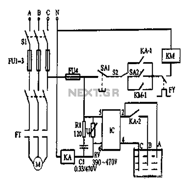
An automatic water tank system is illustrated in the circuit diagram. The circuit employs a PSSR AC solid-state relay, which is a new type of solid-state relay designed for AC applications. Unlike traditional solid-state relays (SSR), this PSSR not...
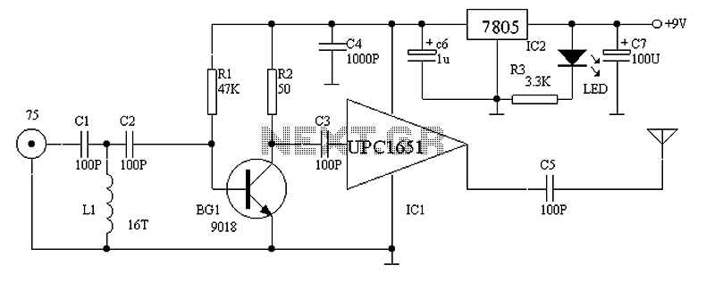
Circuit Overview Many families now own various electronic devices such as televisions, VCD players, video recorders, game consoles, cameras, and DVDs. This circuit involves an RF signal repeater designed to work with a television signal transmitter, covering a radius...
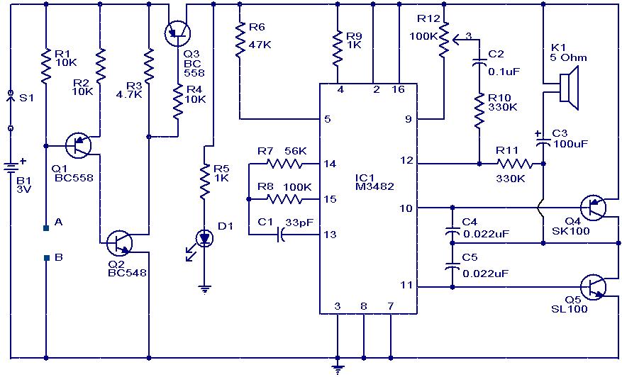
This circuit is a simple musical alarm that generates a tone when water or another conductive liquid touches the two sensor wires provided. It utilizes four transistors and a melody generator integrated circuit (IC) M3482. When water bridges the...

This is a UHF band TV antenna preamplifier circuit with a gain of 15 dB, built using a BF180 UHF transistor. The circuit is straightforward in design. The operational principle consists of two stages. The first stage features a...
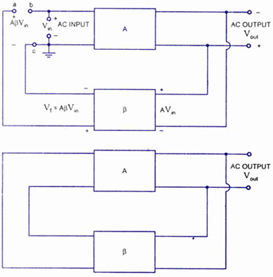
A feedback amplifier with a closed-loop gain, Af, greater than unity can be achieved through the use of positive feedback. This condition also fulfills the phase requirement, leading to the operation of an oscillator circuit. An oscillator circuit generates...