
Variable-duty-cycle-oscillator
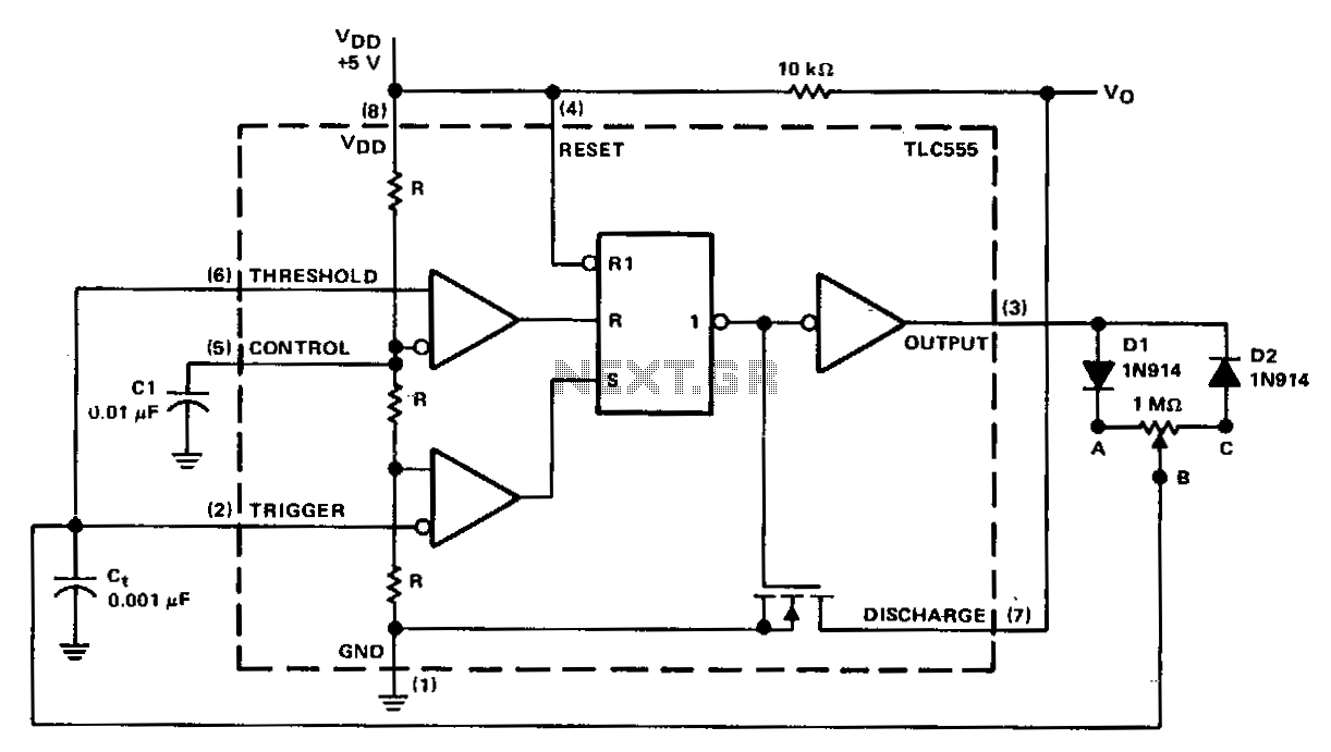
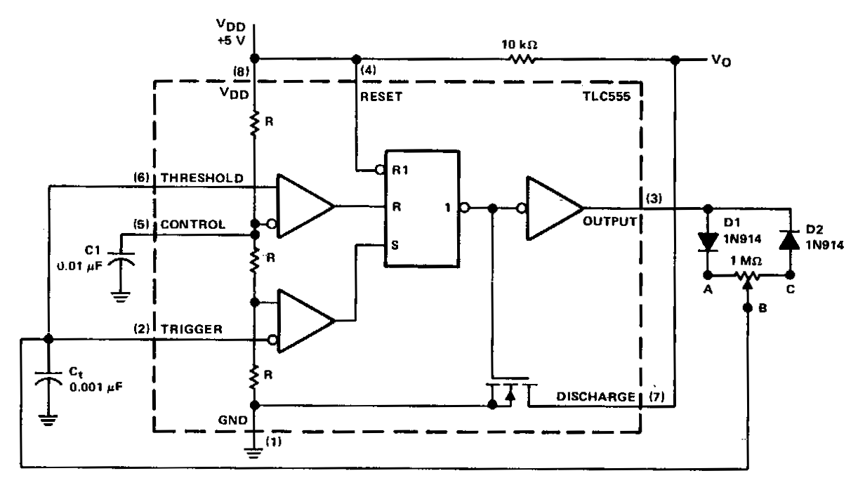
In a basic astable timer configuration, timing periods 11 and 12 are not independently controlled. This lack of control complicates the maintenance of a constant period, T, when either 11 or 12 is varied. In this circuit, the charge resistance RAB and discharge resistance R8c are determined by the position of the common wiper arm of the potentiometer. Therefore, it is possible to adjust the duty cycle by proportionately adjusting 11 and 12 without changing the period T. At start-up, the voltage across capacitor C1 is less than the trigger level voltage (1/2 VDD), causing the timer to be triggered via pin 2. The output of the timer at pin 3 increases, turning off the discharge transistor at pin 7 and allowing C1 to charge through diode D1 and resistance RAB. When capacitor C1 charges to the upper threshold voltage (2/3 VDD), the flip-flop is reset, and the output at pin 3 decreases. Capacitor C1 then discharges through diode D2 and resistor R8c. When the voltage at pin 2 reaches 1/3 VDD, the lower threshold or trigger level, the timer triggers again, and the cycle is repeated. In this circuit, the oscillator frequency remains fixed, and the duty cycle is adjustable from less than 0.5% to greater than 99.5%.
The described astable timer circuit operates using a 555 timer IC, configured to function as an oscillator. The primary components involved include two resistors (RAB and R8c), a capacitor (C1), and two diodes (D1 and D2). The resistors govern the charge and discharge paths of the capacitor, while the diodes ensure that current flows in the correct direction during the charge and discharge phases.
The timing intervals, defined by the resistors and capacitor, can be manipulated by adjusting the potentiometer's wiper arm, which alters the resistance values seen by the circuit. This adjustment allows for fine-tuning of the duty cycle, enabling the circuit to maintain a consistent frequency while varying the proportion of time spent in the high and low output states.
Upon initial power-up, the capacitor C1 begins in a discharged state, with its voltage below the trigger threshold. When the timer is triggered via pin 2, the output at pin 3 transitions to a high state, which deactivates the discharge transistor connected to pin 7. This allows capacitor C1 to charge through resistor RAB and diode D1. The charging continues until the voltage across C1 reaches the upper threshold of 2/3 VDD, at which point the internal flip-flop of the 555 timer resets, causing the output at pin 3 to drop.
Following this, capacitor C1 discharges through resistor R8c and diode D2. The discharge continues until the voltage at pin 2 drops to the lower threshold of 1/3 VDD, triggering the timer again and restarting the cycle. The fixed oscillator frequency, combined with the adjustable duty cycle, makes this configuration suitable for various applications, including pulse width modulation (PWM) and timing applications in electronic circuits. The ability to adjust the duty cycle from less than 0.5% to greater than 99.5% provides significant flexibility for designers in tailoring the circuit's performance to meet specific requirements.In a basic astable timer, configuration timing periods 11 and 12 are not controlled independently. The lack of control makes it difficult to maintain a constant period, T, if either 11 or 12 is varied. In this circuit, charge RAB and discharge R8 c resistances are detenriined by the position of common wiper arm~ of the potentiometer.
So, it is possible to adjust the duty-cycle by adjusting 11 and 12 proportionately, without changing period T. At start-up, the voltage across C, is less than the trigger level voltage ("12 VDD). causing the timer to be triggered via pin 2. The output of the timer at pin 3 increases, turning off the discharge transistor at pin 7 and allowing C, to charge through diode Dl and resistance RAB· When capacitor C1 charges to upper threshold voltage 213 VDD. the flip-flop is reset and the output at pin 3 decreases. Capacitor C, then discharges through diode D2 and resistor R8c. When the voltage at pin 2 reaches 1/3 VnD, the lower threshold or trigger level, the timer triggers again and the cycle is repeated.
In this circuit, the oscillator frequency remains fixed and the duty cycle is adjustable from less than 0.5% to greater than 99.5%. 🔗 External reference
Related Circuits
In a basic astable timer, the timing periods 11 and 12 are not independently controlled. This lack of control complicates the maintenance of a constant period, T, if either 11 or 12 is varied. In this circuit, the charge...
Warning: include(partials/cookie-banner.php): Failed to open stream: Permission denied in /var/www/html/nextgr/view-circuit.php on line 713
Warning: include(): Failed opening 'partials/cookie-banner.php' for inclusion (include_path='.:/usr/share/php') in /var/www/html/nextgr/view-circuit.php on line 713