
Visible-red-continuous-laser-gun

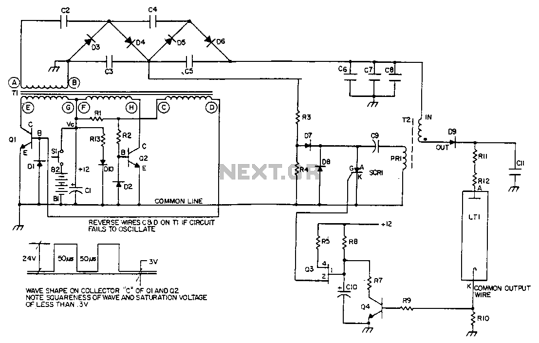
Q1 and Q2 control the primary windings of transformer T1 using a square wave signal, the frequency of which is determined by the magnetic properties of the transformer. Diodes D1 and D2 serve as base return paths for the feedback current of Q1 and Q2. The output winding of T1 is connected to a multi-section voltage multiplier, which is composed of capacitors C1 through C5 and diodes D3 through D6. Resistors R3 and R4 are used to divide the 800 V obtained at the junction of C3 and C5, which is utilized for charging the dump capacitor C9 in the ignitor.
In this circuit, Q1 and Q2 are typically configured as bipolar junction transistors (BJTs) or MOSFETs, depending on the design requirements and switching speed. The square wave signal generated at the primary side of transformer T1 is crucial for efficient energy transfer to the secondary side. The frequency of this square wave is influenced by the inductance and core material of T1, which affects how quickly the magnetic field can build and collapse.
Diodes D1 and D2 are essential for maintaining the correct biasing of Q1 and Q2, ensuring that they operate in the desired switching regime without experiencing undue stress or thermal issues. The feedback mechanism provided by these diodes allows for stable operation and helps regulate the output voltage levels.
The voltage multiplier circuit formed by capacitors C1 through C5 and diodes D3 through D6 serves to increase the voltage generated by the output winding of T1. Each stage of the multiplier effectively doubles the voltage, allowing for high voltage outputs suitable for applications such as ignitors. The capacitors are charged during the positive half-cycles of the square wave, while the diodes prevent reverse current flow, ensuring that the capacitors retain their charge.
Resistors R3 and R4 play a critical role in voltage division, allowing a portion of the high voltage (800 V) to be safely utilized for charging the dump capacitor C9. This capacitor is used in the ignitor circuit to store energy for a rapid discharge, which is necessary for ignition applications. Proper selection of resistor values is important to ensure that the voltage across C9 is within the required range for reliable operation.
The overall design of this circuit emphasizes efficiency and reliability, utilizing components that can handle high voltages and currents while maintaining stable operation under varying conditions. Careful attention to the layout and component selection is necessary to minimize losses and ensure safe operation.Ql and Q2 switch the primary windings of transformer Tl via a square wave at a frequency determined by its magnetic properties. Diodes Dl and D2 provide base return paths for the feedback current of Ql and Q2. The output winding of T1 is connected to a multiple section voltage multiplier. That multiplier consists of capacitors Cl through C5 and diodes D3 through D6. Resistors R3 and R4 divide the 800 V taken off at the junction of C3, and C5 for charging the dump capacitor C9 in the ignitor.
🔗 External reference
Related Circuits
Q1 and Q2 control the primary windings of transformer T1 using a square wave at a frequency determined by the transformer's magnetic properties. Diodes D1 and D2 provide return paths for the feedback current of Q1 and Q2. The...