
Voltage Multiplier
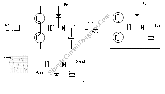
A voltage multiplier circuit is designed to increase the voltage level of an input signal, typically a square wave, by utilizing capacitors and diodes to achieve the desired output. In this specific configuration, the circuit doubles the amplitude of the input square wave. The basic operation involves charging capacitors during one half of the waveform and discharging them to the load during the other half.
The circuit typically consists of a series of diodes and capacitors arranged in a specific topology. For instance, in a simple two-stage voltage doubler, the first diode allows current to flow into the capacitor during the positive half-cycle of the input waveform, charging it to the peak voltage minus the forward voltage drop of the diode. During the negative half-cycle, the charged capacitor discharges through the load, effectively doubling the output voltage.
It is important to note that there is a voltage drop associated with the base-emitter junction of transistors present in the circuit. This drop is typically around 2V, which must be accounted for in the design to ensure that the output voltage meets the required specifications. The overall efficiency of the circuit can be affected by these losses, and careful selection of components can help mitigate them.
Additional considerations for optimizing performance include selecting diodes with low forward voltage drops and capacitors with appropriate voltage ratings to handle the increased output voltage. The load connected to the output should also be considered, as it will influence the overall behavior of the circuit and its ability to maintain the desired output voltage under varying conditions. Proper thermal management may also be necessary to ensure reliability and longevity of the components used in the circuit.This is a voltage multiplier circuit. First circuit is used to double the a square wave (any amplitude). However there is minus about 2v losses in base-emitter.. 🔗 External reference
Related Circuits
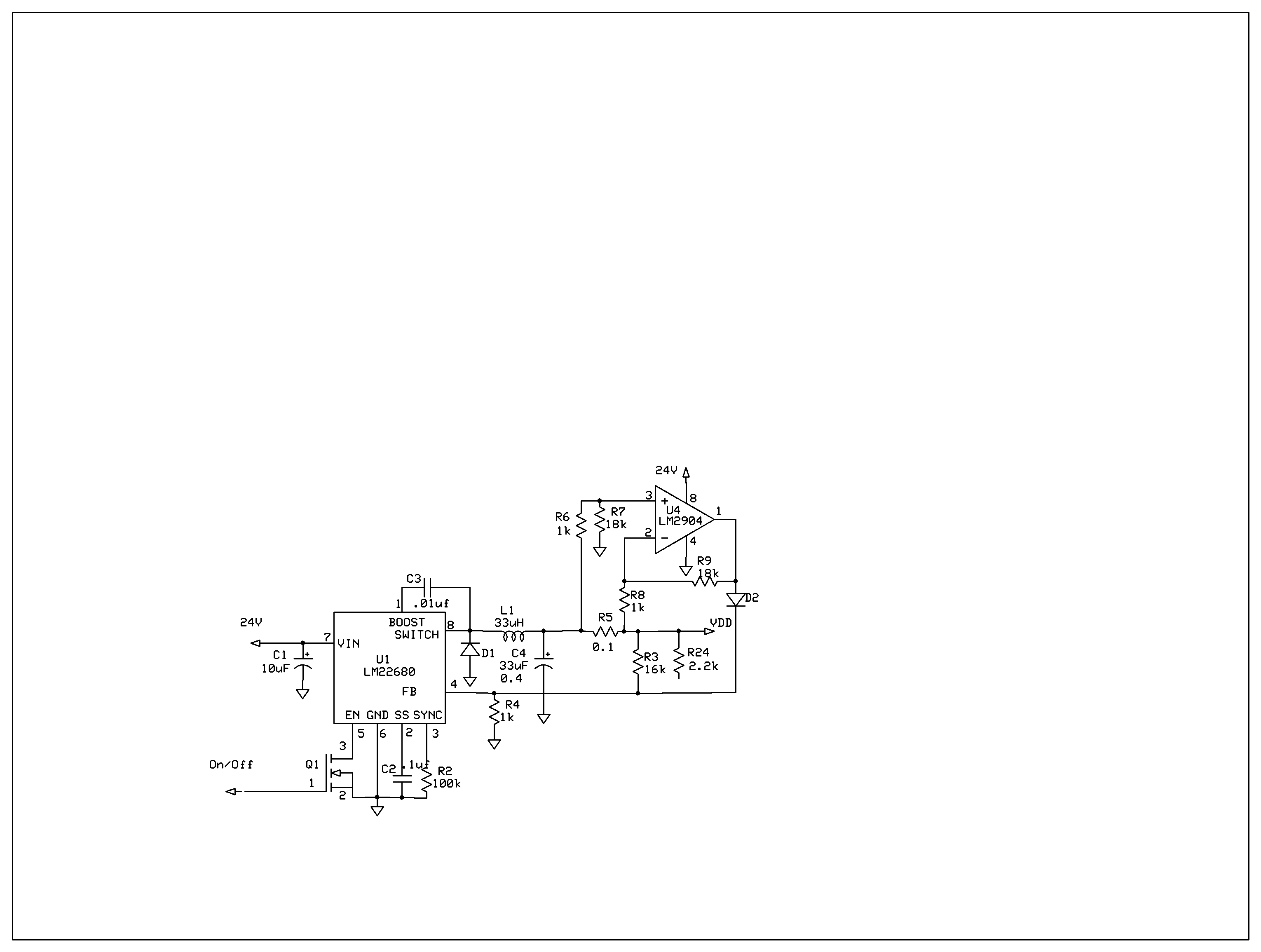
The product requires a voltage-controlled, current-limited power supply. Various switcher chips have been used with an op-amp to provide feedback for a current sense voltage to the feedback pin. Currently, an LM22680 is in use, but it has shown...

A voltage-controlled oscillator (VCO) operates similarly to a voltage-to-frequency converter (VFC). Its output frequency is determined by a control voltage input. In the circuit diagram, 'd' represents the amplifier input voltage, which is set to 0.6V, while 'h' denotes...

A ripple-free, short-circuit protected variable output voltage and current power supply is presented on this website as a verified project. The circuit diagram includes a description of various power supply circuits. This power supply circuit is designed to provide a...
The NJM2670 is a general-purpose 60V dual H-bridge drive integrated circuit (IC). It features a pair of H-bridges, a thermal shutdown circuit, and an alarm output. The alarm output is capable of detecting application issues, thereby significantly enhancing system...
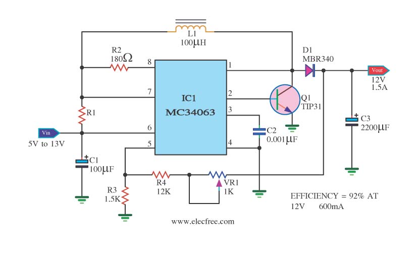
The circuit is a battery-powered voltage regulator that outputs 12V at 1.5A. It accepts an input voltage range from 5V to 13V. The circuit utilizes the MC34063 integrated circuit, making it a straightforward design. The circuit primarily functions as a...
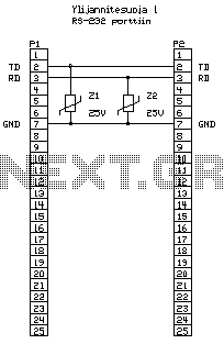
RS-232C serial port lines are quite prone to be damaged by overvoltages. The damage to computer serial ports has become more and more expensive to replace because of higher integration: usually, you have to buy a new motherboard if...