
Wogglebug circuit
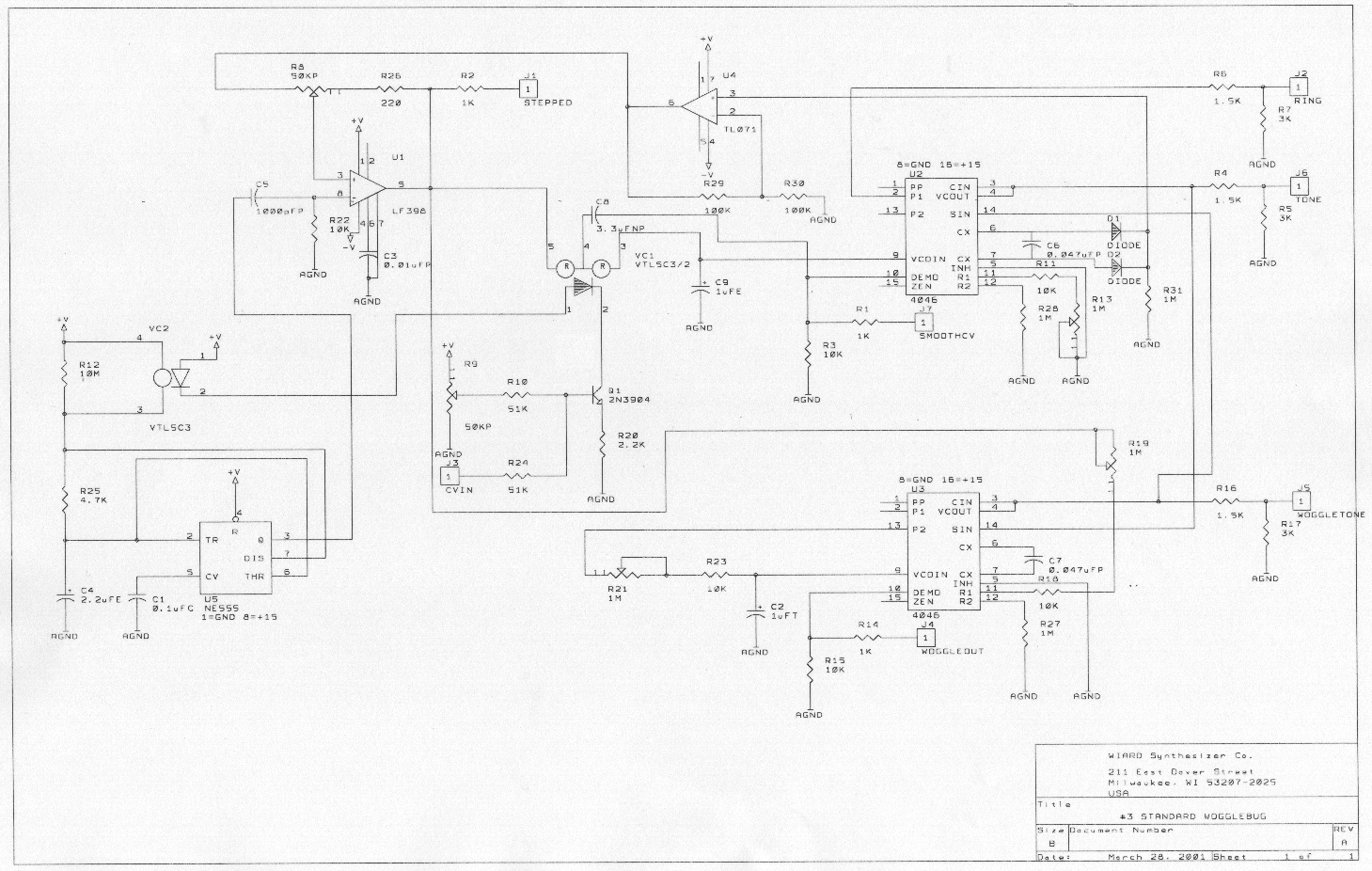
The circuit described incorporates a 555 timer integrated circuit, which is widely utilized in various timing and oscillation applications. The addition of a second RM output enhances the versatility of the circuit, allowing for multiple output signals that can be synchronized or modulated. The sync input, derived from a voltage-controlled oscillator, enables the 555 timer to operate in conjunction with other oscillators, facilitating synchronized operations in modular synthesizer setups.
The mention of unspecified transistors indicates that further investigation is necessary to identify their roles within the circuit. The Wiard schematics, which provide essential details for the circuit's layout and functionality, should be consulted for clarification. The VCO3 circuit may also contain relevant information regarding the unidentified transistor.
Capacitor designations are critical for ensuring proper functionality. The standard classifications of capacitors (ceramic, poly, tantalum) indicate the materials used and their respective properties, which can affect performance in timing and filtering applications. The 'FP' and 'NP' designations warrant further investigation to understand their significance in this context.
The unassigned pads on the PCB suggest potential locations for additional connections, possibly for voltage returns associated with potentiometers. The configuration near the LF398, which connects to ground and V-, should be verified to ensure it aligns with the intended circuit design. The identification of potentiometer names is crucial for proper integration and functionality, particularly when working from a block diagram that may not provide comprehensive details.
The mention of Grant's production model highlights the evolution of the design, with enhancements that may not be documented in earlier schematics. The inclusion of disturbance CVs and LEDs indicates an effort to expand the module's capabilities, providing users with more control and visual feedback.
The Wogglebug circuit represents a more complex iteration of the basic module, incorporating additional features that enhance its functionality within a synthesizer context. The use of a second LF398 suggests a more intricate design that could improve signal processing or modulation capabilities.
For those interested in modifications or enhancements, resources such as the Wiardgroup on Yahoo provide community-driven insights and additional circuits designed by experienced users. These can serve as valuable references for expanding the functionality of the Wogglebug or similar modules.
Overall, the circuit presents a rich platform for experimentation and development, with opportunities for customization and enhancement through careful analysis of the schematics and available resources.I added a second RM output and a sync input to the 555. The latter is based off of one of Rene Schmitz VCOs. ( ) ok, thank you. i asked because on the two PCB pictures above there are e. g. two transistors without any specification. the wiard schematics contains one of them and the other one i guess i`ll have to look for in the VCO3 circuit you mentioned. ok, thank you. i asked because on the two PCB pictures above there are e. g. two transistors without any specification. the wiard schematics contains one of them and the other one i guess i`ll have to look for in the VCO3 circuit you mentioned. As far as the capacitor types go i am resonably comfortable that C denotes ceramic, P is poly (-styrene -ester -propelyene ), T is tantalum.
But what give with the FP and NP designations There are 4 pairs of pads left blank, I am imagining that several are for returns to V+/- and ground for some of the pots Is this correct There is a pair open just north of the 398, one side grounded the other jumpered to V-. Does anyone have a handy list of the names for the potentiometers I have been trying to work it out from the block diagram on the Wiard site to no avail.
It would also seem that Grant`s production model has a good bit more packed into it than his basic schem shows, such as the disturb CVs and a bunch of lovely LEDs. any leads on these extras As far as the capacitor types go i am resonably comfortable that C denotes ceramic, P is poly (-styrene -ester -propelyene ), T is tantalum.
But what give with the FP and NP designations There are 4 pairs of pads left blank, I am imagining that several are for returns to V+/- and ground for some of the pots Is this correct There is a pair open just north of the 398, one side grounded the other jumpered to V-. Does anyone have a handy list of the names for the potentiometers I have been trying to work it out from the block diagram on the Wiard site to no avail.
It would also seem that Grant`s production model has a good bit more packed into it than his basic schem shows, such as the disturb CVs and a bunch of lovely LEDs. any leads on these extras The Wiard production Wogglebug is a more sophisticated version. I tried working out what was behind the front panel at some point. not sure where my notes are for that. I`m pretty sure a second LF398 is involved. I`ll see if I can find my stuff. Obviously, Grant isn`t going to give out his secret recipe. Despite the fact that the Wogglebug #3 is simpler than the production version, it is still a fantastic module.
You could always start with that and hack other stuff onto it. The Wiardgroup on yahoo groups has some extra add-onn circuits that Dr. Mabuse designed. Might want to check those out. These are good questions. I never realized that people would be interested in this layout, which is why the parts placement is still in its cryptic format. I`ll try to whip up one that`s more user friendly. This is definitely not right. I already checked the PCB for obvious errors or solder where it should not been. found some, fixed all. still the same problem. 🔗 External reference
Related Circuits
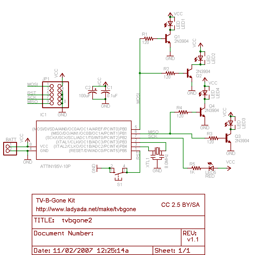
Why use one resistor and one transistor for each LED instead of connecting the LEDs in series and controlling them with a single transistor? This approach is controlled by an Arduino pin through a single resistor. While there is...

This electronic game pits a human player against the machine. The opponents use a common game token and take turns moving along a path by one, two, or three steps, with the winner being the first to reach the...
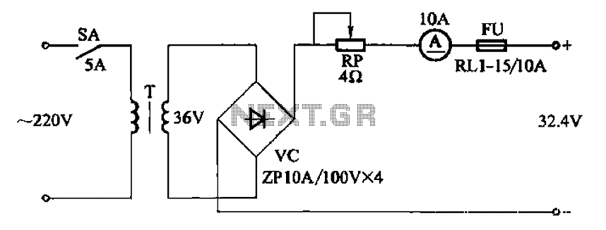
The adjustment potentiometer RP can modify the charging current. The adjustment potentiometer, designated as RP, serves a critical role in regulating the charging current within an electronic circuit. This component is typically a variable resistor that allows for fine-tuning of...
This inverter circuit is designed to power electric razors, stroboscopes, flash tubes, and small fluorescent lamps using a 12-volt car battery. Unlike typical feedback oscillator inverters, this design features a separate oscillator from the output stage, allowing for easy...
The key to avoiding instability (motor-boating) in a high-gain circuit is to power the speaker using a separate power supply. This circuit design allows for the connection of one or two additional stations. It is recommended to construct the...
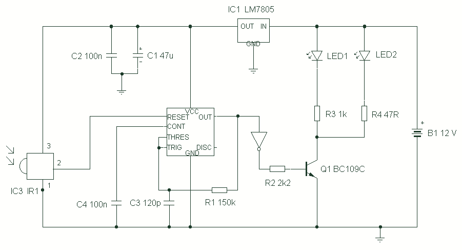
IR appliances use pulses (control signals) sent over a modulated IR carrier wave. The carrier wave may be modulated at various frequencies, 36-38KHz being the most popular. Some Satellite receivers use even higher frequencies than this. The IR1 remote...