
Low-noise switching power supply schematic circuit diagram

The circuit operates by first converting an AC input into a DC voltage using the rectifying components. The arrangement of R1, L1, D1, and the capacitors (C1 to C7) ensures that the voltage is smoothed and filtered to achieve the desired 30V output. The LC filter on the right, consisting of L5 and C11, further refines the output by attenuating any high-frequency noise that may have been introduced during the conversion process.
The feedback mechanism, facilitated by IC2, D8, R9, and R10, plays a crucial role in maintaining voltage regulation. The feedback loop monitors the output voltage and adjusts the switching elements of the DC-DC converter to ensure that the output remains stable under varying load conditions. This closed-loop control is essential for applications where voltage stability is critical.
In the central section of the circuit, careful attention is given to noise management. This may involve the use of additional filtering components or layout considerations to minimize electromagnetic interference (EMI) and ensure that the circuit operates efficiently. Proper disposal of noise is vital for the reliability of the power supply, particularly in sensitive electronic applications.
Overall, this circuit design emphasizes efficient power conversion, stable output voltage, and effective noise reduction, making it suitable for various applications requiring reliable DC power. Circuit shown in Figure, the circuit can achieve greater power output, just change the part of the device. FIG circuit R1 to the left, L1, D1, C1 to C7 are conventional common mode filtering and rectifying circuit to obtain a DC voltage of about 30V DC-DC converter circuit for use; rightmost circuit L5, C11 and other ordinary LC filter circuit; IC2, D8, R9, R10 voltage feedback circuit composition, form a closed loop structure, stable power supply output voltage; the middle part of the DC-DC converter, the key to reducing noise in this circuit is a part of proper disposal.
Related Circuits
The TEA5764UK is a single-chip, electronically tuned FM stereo radio that includes a Radio Data System (RDS) and Radio Broadcast Data System (RBDS) demodulator, along with an RDS/RBDS decoder. This device is designed for portable applications and features fully...
The TMS320C6678 DSP is a component of the DSP based on the KeyStone framework recently released by Texas Instruments. It features 8 cores and achieves operating speeds that can reach up to 10 GHz. However, it has high power...
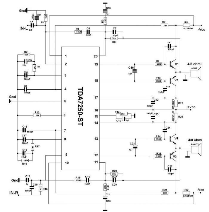
The TDA7250 audio driver, manufactured by SGS Thomson, can be utilized to design a straightforward high-power audio amplifier project with minimal external components. This audio amplifier can operate with either a 4-ohm or an 8-ohm load, delivering a maximum...
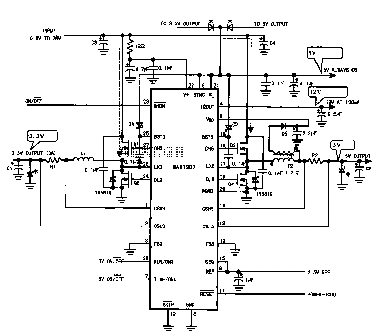
Multi-output power supply circuit (MAX1902). This circuit illustrates the power supply configuration for a notebook computer motherboard, utilizing the MAX1902 chip for power control. It is designed to convert the battery's DC voltage into multiple DC voltage outputs. The multi-output...
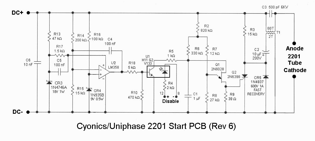
This chapter provides detailed schematics of various power supplies suitable for use with common Ar/Kr ion tubes available to hobbyists in the surplus market. Included are examples of commercial designs (Omnichrome 150R and 532 head, Lexel 88 and head)...

The circuit of the unit is fairly simple, but is a bit irksome to set up. The reason is that obtaining matched FETs is not easy, so I had to make sure that the circuit would work with off-the-shelf...