
0-40V lab power supply circuit diagram electronic project using LM723 L146
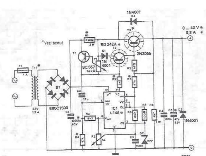
The adjustable laboratory power supply circuit is designed to provide a versatile and reliable source of DC voltage for various electronic applications. The LM723 voltage regulator is a well-established component known for its ability to maintain a stable output voltage, while the L146 offers enhanced performance for higher voltage applications. The circuit is configured to allow for fine-tuning of both voltage and current outputs, making it suitable for testing and powering a wide range of devices.
The circuit diagram highlights the integration of a resistive network that effectively mitigates the minimum output voltage limitation typically associated with integrated circuits. By employing potentiometer P2, users can achieve a full range of output voltages down to zero, which is particularly beneficial for applications requiring precise voltage control.
The choice of capacitors in the circuit is critical as they must be selected based on the required output characteristics, including ripple voltage and load stability. Additionally, the power dissipation must be carefully monitored to ensure that the transistors do not exceed their thermal limits. The inclusion of parallel 2N3055 transistors allows for greater current handling capabilities, which is essential when powering devices that require higher currents. This configuration, however, demands a transformer capable of supplying sufficient current, thereby ensuring the overall stability and reliability of the power supply.
In summary, this adjustable power supply circuit is a robust solution for laboratory environments, providing flexibility in voltage and current outputs while ensuring safe operation through careful component selection and configuration.A very lab adjustable power supply that can provide an output voltage between 0 and 60 volts can be designed using this circuit diagram. This lab power supply can be designed with LM723 chip or for higher output voltages, with L146. Output current is also adjustable, but once established, is always effective. Table 1 shows the values to be modif ied to have three different versions of the maximum output voltage (30, 40 and 60 V). Electrical diagram below shows the alternative 40 V / 0. 8 using L146 chip because it can stabilize higher output voltage, much better than the LM723. Normally, 2 V is the minimum voltage stabilized that even an integrated circuit can provide. Resistive network R3, R4 and R5, R6 "kill" this restriction so that output can be set to 0 V with potentiometer P2. Depending on the output requirements, will be decided on the type and the semiconductor capacitors to be used.
Output current must be limited so as to keep power dissipation of 40 W. T3 under maximum output current for 40 V version is 0. 8 A. It can connect two parallel 2N3055 transistors (with emitter resistors) to double the current output, but in this case requires a 2 A transformer 🔗 External reference
Related Circuits
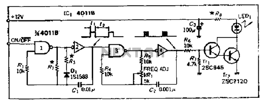
The 4000 Series 4011B is a NAND gate used in conjunction with a 4AI NAND gate circuit group to create two loops of an unstable multivibrator. The first NAND gate and the second NAND gate operate at approximately 1...
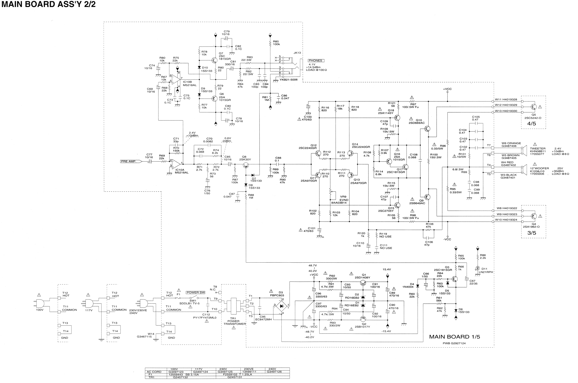
Some resistors on the circuit board of a Roland KC-300 amplifier have burned out and are so charred that their specifications cannot be determined. The resistors in question are R82, R83, R85, R92, and R93. Resistors R92 and R93...
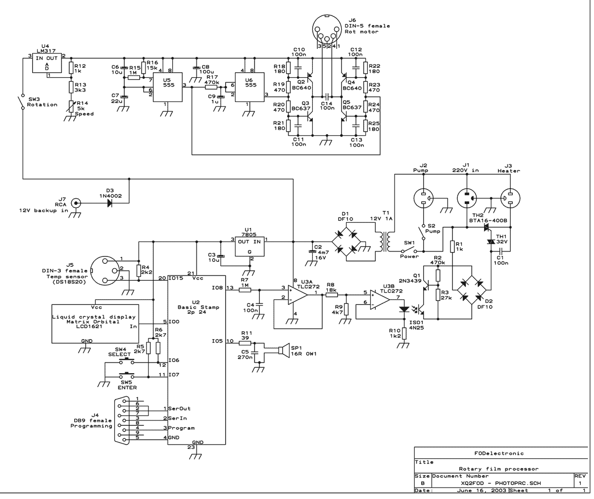
This machine essentially does three things: It controls the process temperature, provides constant agitation of the chemical baths, and performs the timing. The operator must pour in and out the liquids by hand. The heart of the circuit is...
Protect your LCD or Plasma TV with this small delay-on circuit. The SMPS-based power supply of these modern electronic devices is susceptible to voltage spikes. This delay-on circuit is designed to enhance the protection of LCD and Plasma TVs by...
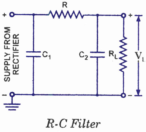
The disadvantages of pi-filters include higher costs, increased weight, larger size, and the external magnetic field generated by the series inductor. These issues can be mitigated by substituting the series inductor with a series resistor, referred to as an...

The ICL7107 is a 3 1/2 digit LED analog-to-digital converter (A/D converter). It features an internal voltage reference, high-isolation analog switches, sequential control logic, and display drivers. The ICL7107 is designed to convert analog signals into digital representations with a...