
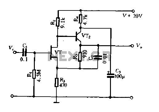
100w basic mosfet amplifier

Parts list:
C1 = 2.2 µF MKP, MKT 100 V
C2 = 330 pF ceramic 50 V
C3 = 100 nF MKP, MKT 100 V
C4 = 40 µF 100 V electrolytic
C5, C6 = 18 pF ceramic 50 V
C7 = 100 nF MKP, MKT 250 V
C8 = 47 µF 100 V
R1 = 47 K
R3 = 470 Ohms
R2 = 2.2 K
R4, R5 = 3.9 K
R6 = 1 K
R7 = 27 K
R8, R9, R11 = 100 Ohms
R10 = 10 K
R12, R13 = 470 Ohms
R14, R15 = 0.33 Ohm 5 watts
R16 = 10 Ohm 3 watts
R17 = 1 K
R18, R19 = 10 K
T1, T2, T9, T10 = 2N5401, ZTX558, BC556B (note the different pinout - take care for pin layout)
T3, T4 = BF470, MJE350, 2SB649
T5, T6 = BF469, MJE340, 2SD669
T7 = IRFP240, 2SK1530, 2SJ162, BUZ900DP, BUZ901DP (note the different pinout - take care for pin layout: GDS GSD)
T8 = IRFP9240, 2SJ201, 2SK1058, BUZ905DP, BUZ906DP (note the different pinout - take care for pin layout: GDS GSD)
P1 = 100 Ohms (25 laps - 25 turns)
P2 = 2K5 (25 laps - 25 turns)
F1, F2 = 3 A
The circuit design of this MOSFET amplifier emphasizes simplicity and efficiency, making it suitable for various audio applications. The use of MOSFETs for output stages allows for high linearity and low distortion, crucial for high-fidelity audio reproduction. The differential stages formed by T1, T2, T5, and T6 ensure that the input signal is amplified with minimal noise, contributing to the overall sound quality. The current mirror configuration provided by T3 and T4 stabilizes the operation of the differential amplifiers, allowing for consistent performance across varying load conditions.
Fine-tuning the output DC voltage with P1 is essential for optimal performance, as it helps mitigate potential DC offset issues that could affect connected speakers. The quiescent current adjustment through P2 is also critical, as it influences the thermal stability and efficiency of the output stage. The specified thermal resistance of the heatsink ensures effective heat dissipation, preventing thermal runaway and prolonging the lifespan of the MOSFETs.
The inclusion of short-circuit protection via F1 and F2 adds a layer of safety, safeguarding the amplifier and connected components from damage due to unexpected load conditions. The specified power supply voltage range ensures that the amplifier operates within its designed parameters, providing the necessary headroom for dynamic audio signals.
Overall, this MOSFET amplifier design exemplifies a balance between performance and simplicity, making it accessible for both hobbyists and professionals looking to create high-quality audio amplification systems.This Basic MOSFET amplifier is very simple to build and low cost. Is perfect for Hi-Fi amplifiers and instrument amplifiers (guitar, keyboards ). Output power is + / 100 Wrms at 8 ohm load or + / 160 Wrms below 4 ohms. The simplicity of this circuit cause distortion + / -0. 1%. Bandwidth at -3 dB is from 4 Hz to 96 Khz and it is limited by C1, R1, R2 and C2. Transistors T1 and T2 makes a first differential stage, current source of +/- 1 mA is set by R3. P1 allows a fine tuning of DC voltage at amplifier`s output. Place P1 at it`s half value for first power up, then turn it slowly for a lowest DC output voltage. It is recommended to use a first quality component. Input sensitivity is 1. 2 volts. The gain of 27x is archived by R7/R6. It may be modified by changing R7 value. Transistors T5 and T6 makes the second differential stage. Transistors T3 and T4 works as a current mirror source. They push the second differential stage to drain equal current. Doing so we get a high gain and an excellent linearity. Output MOSFET transistors works in AB class, their quiescient current is set from 50 to 100 mA trough P2. For setting quiescient current, you must set P2 in minimal resistance, place a multimeter in mV DC range accross on R14 or R15 leads, turn slowly the screw untill you read a 16, 5 mV value, which correspond to a 50 mA quiescient current.
F1 and F2 works as an elementary output short-circuit protection. The power supply must have a value between 45 and 55 Volts DC (positive and negative). One heatsink with a thermal resistance less of 2 ° C / W is required. All resistors are 1% metal film 1/4 watt. Before connecting a speaker at amplifier output, connect a multimeter at output and look on DC output voltage. This level never may be greater than 50 mV. If it is so, check all amplifier for a mistake. Also, change T2 with another device and check again. Parts list : C1 = 2. 2 uF MKP, MKT 100 V C2 = 330 pF ceramic 50 V C3 = 100 nF MKP, MKT 100 V C4 = 40 uF 100 V electro-chemical C5, C6 = 18 pF ceramic 50 V C7 = 100 nF MKP, MKT 250 V C8 = 47 uF 100 V) R1 = 47 K R 3 = 470 Ohms R2 = 2K2 R4, R5 = 3K9 R6 = 1 K R7 = 27 K R8, R9, R11 = 100 ohms R10 = 10 K R12, R13 = 470 ohms R14, R15 = 0.
33 ohm 5 watts R16 = 10 ohm 3 watt R17 = 1 K R18, R19 = 10K T1, T2, T9, T10 = 2N5401, ZTX558, BC556B (note the different pinout - take care for pin layout) T3, T4 = BF470, MJE350, 2SB649 T5, T6 = BF469, MJE340, 2SD669 T7 = IRFP240, 2SK1530, 2SJ162, BUZ900DP, BUZ901DP (note the different pinout - take care for pin layout: GDS GSD) T8 = IRFP9240, 2SJ201, 2SK1058, BUZ905DP, BUZ906DP (note the different pinout - take care for pin layout: GDS GSD) P1 = 100 ohms (25 laps - 25 turns) P2 = 2K5 (25 laps - 25 turns) F1, F2 = 3 T A 🔗 External reference
Related Circuits

This audio amplifier circuit, connected to 32 Ohm impedance mini-earphones, can detect very remote sounds. Useful for theatre, cinema and lecture goers: every word will be clearly heard. You can also listen to your television set at a very...
The Field Effect Transistor (FET) exhibits a high input impedance, allowing the construction of high input impedance amplifiers. However, as a FET amplifying device, the distributed capacitance and the Miller effect significantly increase input capacitance at high frequencies. Furthermore,...

This circuit utilizes a MOSFET amplifier as the primary component for boosting audio signals. It is designed to drive a speaker with an impedance of 8 Ohms and a power output exceeding 200W. Additionally, a suitable power supply circuit...
There is no substitute for sheer power—low-efficiency speakers, outdoor sound systems, or perhaps the full dynamic range of a high-power amplifier. Whatever the requirement, this super power module should meet the needs. The amplifier can be divided into three...
The NE5532 preamplifier is widely recognized for its excellent performance. It is now being utilized as a small power amplifier. While the general operational amplifier (op-amp) circuit remains similar, there are notable changes in some resistors and capacitors, leading...
This is a video amplifier circuit or video splitter circuit, designed to strengthen video signals. It compensates for signal loss and is... The video amplifier circuit serves as a crucial component in video signal distribution systems, ensuring that the integrity...