
120W power amplifier circuit

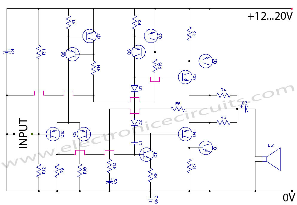
The described amplifier circuit utilizes a floating power supply to enhance output power capabilities, making it suitable for various applications where increased amplification is required. The use of an input voltage follower configuration (ICLA) ensures that the circuit maintains high input impedance, which is critical for interfacing with different signal sources without loading them down. The design's stability is further reinforced by the all-transistor closed-loop architecture, which minimizes the risk of self-oscillation and allows for high open-loop gain.
The inclusion of a capacitor (C4) at the non-inverting terminal of ICLB is particularly noteworthy, as it serves to extend the frequency response of the amplifier. This characteristic is essential for applications that demand fidelity across a broader frequency range, such as audio amplification or RF signal processing. The floating power loop established by components R6, C6, and C7 supports the operational amplifier's performance, ensuring that it can operate effectively within the desired frequency range.
The output stage bias circuit, composed of VT1, VT2, R7, R8, and R9, is designed to maintain optimal operating conditions for the output transistors. This biasing arrangement is crucial for preventing thermal runaway and ensuring consistent performance under varying load conditions. The gate protection circuit formed by F_T and F_KU provides an additional layer of safety for the output transistors, safeguarding them against voltage spikes that could lead to damage.
Overall, the amplifier circuit's design principles and component choices reflect a comprehensive approach to achieving high performance, stability, and versatility in amplification applications.Amplifier circuit of this paper is to introduce a floating power supply, the purpose is to increase the output power, the amplifier output power with only the final stage ampli fier supply voltage and casts about. Its principle is shown 2--116 shown. Iclt) as a pre-stage, ICla composition as the input voltage follower circuit, the purpose is to increase the input impedance, and to facilitate a variety of sources are connected. Its voltage gain of 1, is conducive to stable operation of the circuit o circuit input is suspended, the power stage, IClb inverting input voltage follower Icl group also be suspended.
This circuit is equivalent to the whole big closed loop of all-trans -fed, or that the whole closed loop of l, which makes the circuit very stable and, in any case does not appear self-excited. Closed loop feedback in turn means that the whole machine high open loop gain, the open loop gain of the unit up to lOOdB above.
Therefore, even if the final stage amplifier tube mismatch, it also minimal distortion oIClb noninverting terminal of the capacitor C4 is introduced to broaden the high frequency band, so that it reaches 60kHZo where ~ R6, C6, C7 op amp IClb floating power loop, vTl, VT2 and R7 ~ Rio and RPi, touch 2 group into the output stage bias circuit, f t ~ f Kui form the output pipe gate protection circuit.
Related Circuits
Discrete Class AB Transistor Audio Power Amplifier Circuit Diagram. This is a Class AB transistor power amplifier. It is a simple amplifier to... A Class AB transistor audio power amplifier is designed to provide high-quality amplification for audio signals while...
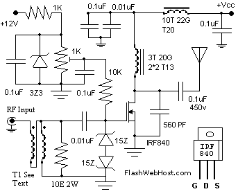
The 60 Watt linear amplifier is a simple all solid-state circuit using power MOSFET IRF840. The IRF series of power transistors are available in various voltage and power ratings. A single IRF840 can handle a maximum power output of...
The input impedance can be classified into high-impedance and low-impedance inputs based on the requirements of various audio equipment and the load impedance. High-impedance input mode is typically utilized in general audio devices such as CD players, VCD players,...

Numerous white LED driver circuits are available, with a well-known design called the Joule Thief capable of powering a single white LED from a 1.2V or 1.5V battery cell. Most of these circuits utilize one or two transistors to...
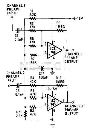
The circuit operates using two 741 operational amplifiers and achieves a gain exceeding 20 dB in each channel. Utilizing a higher-quality op-amp can improve the noise figure and bandwidth. Additionally, the circuit features a sharp roll-off at 20,000 Hertz. This...

This circuit is designed for differential analog circuit switches. The FM1208 monolithic dual differential multiplexer is utilized in applications where the RDS (ON) must be closely matched. The RDS (ON) for the monolithic dual multiplexer operates with a precision...