
27Mhz and 49Mhz rf oscillator-transmitter

The described circuit employs two NPN transistors functioning as a modulator and oscillator, which are integral components in RF (radio frequency) applications. The modulator transistor's base is driven by a bidirectional current source, allowing for controlled modulation of the signal. The high voltage condition is established through a saturating PNP transistor that connects to the voltage regulator (Vreg) at pin 4, ensuring that the modulator operates efficiently within the specified voltage range. Conversely, the low voltage condition is managed by a saturating NPN transistor coupled with a diode to ground, providing a stable reference point for the modulation process.
The oscillator section of the circuit is designed to operate in class C mode, a configuration well-suited for RF transmission due to its high efficiency and ability to produce high-frequency oscillations. The use of third overtone crystals operating at frequencies of 27 MHz or 49 MHz is critical in this design. These crystals are selected for their ability to resonate at specific overtone frequencies, which are multiples of the fundamental frequency, thereby allowing for precise frequency generation.
To ensure that the oscillator operates correctly at the desired frequency, a tuned collector load is implemented. This load is essential for matching the impedance of the oscillator circuit to the load, thereby maximizing power transfer and minimizing reflections. The tuned load typically consists of inductive and capacitive components that create a resonant circuit, allowing the oscillator to maintain stable oscillations at the targeted frequency.
Overall, the combination of a well-regulated modulator and a precisely tuned oscillator circuit is crucial for achieving reliable performance in applications requiring stable RF signal generation. The careful selection of components and configuration ensures that the system meets the stringent requirements of modern communication systems.The modulator and oscillator consist of two NPN transistors. The base of the modulator transistor is driven by a bidirectional current source with the voltage range for the high condition limited by a saturating PNP collector to the pin 4 Vreg voltage and low condition limited by a saturating NPN collector in series with a diode to ground. The crystal oscillator/transmitter transistor is configured to oscillate in a class C mode Because third overtone crystals are used for 27 MHz or 49 MHz applications a tuned collector load must be used to guarantee operation at the correct frequency.
Related Circuits
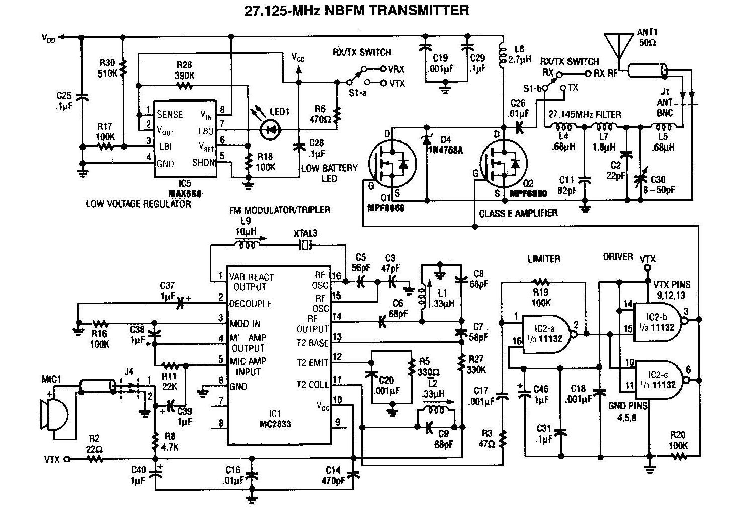
A 27MHz transmitter circuit schematic utilizing the MC2833 and two FET transistors, MPF6660. This design incorporates a Motorola MC2833 one-chip FM transmitter along with several supporting components. The 27MHz transmitter circuit is designed to operate within the FM radio frequency...

This design circuit is for a simple 27MHz transmitter that produces a carrier signal. The circuit generates an unmodulated 27MHz signal, which can be received by a compatible receiver. The transmitter operates as a basic crystal oscillator, with the...
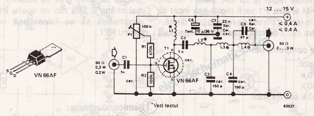
The 10-meter 27MHz continuous wave (CW) radio amplifier is equipped with the VN66AF transistor produced by Siliconix, which offers several advantages: it is inexpensive, provides excellent dielectric insulation, and has high gain. The VN66AF is utilized as an RF...
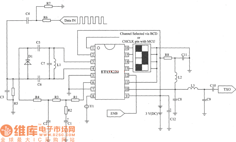
ETl3X220 is a cost-effective single-chip transmitter that operates via RF communication. It supports up to 10 channels and is ideal for applications such as wireless mice, keyboards, and other communication devices. The main technical features include: - Analog FM...
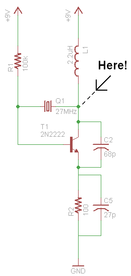
Instead of concentrating on the mathematical and theoretical aspects of this simple pyro RF transmitter, the focus will be on the components within each stage. The mathematics involved in understanding how and why this circuit operates is complex and...

A 27MHz NBFM transmitter circuit schematic featuring the MC2833 and two MPF6660 FET transistors. Utilizing the Motorola MC2833 one-chip FM transmitter along with several supporting components and an MPF6660 RF amplifier, this transmitter can deliver up to 3W into...