
2SC2922 and 2SA1216 or 2SC3264 and 2SA1295 power amplifier circuit

The described amplifier circuit showcases a sophisticated design aimed at delivering high-fidelity audio performance with robust protection mechanisms. The differential input stage ensures that the amplifier can handle a wide range of input signals while maintaining linearity and minimizing distortion. The use of bipolar transistors in conjunction with FET devices for the input stage allows for improved performance characteristics, including lower noise and higher input impedance.
The low-pass filter configuration at the input stage is crucial for reducing unwanted high-frequency noise that could interfere with the audio signal. By carefully selecting the resistor and capacitor values, the circuit designers can tailor the frequency response to suit specific application requirements, thus enhancing the overall sound quality.
The inclusion of an overload protection circuit is essential for safeguarding the amplifier and connected speakers from damage due to excessive signal levels. This feature ensures that the amplifier can operate safely under varying load conditions, providing peace of mind to users who may push the amplifier to its limits.
Furthermore, the speaker protection circuitry is a valuable addition, allowing for a delay in speaker connection after power-up. This delay helps to prevent audible thumps or pops that could occur when the amplifier is first turned on, protecting both the amplifier and the speakers from potential damage.
In summary, this amplifier circuit represents a well-thought-out design that combines advanced electronic components and protective measures to deliver high-quality audio amplification. The attention to detail in the circuit design, from input filtering to output protection, reflects a commitment to achieving optimal performance in high-fidelity audio applications.Amp 2SC2922 and 2SA1216 (or 2SC3264 and 2SA1295) performance is very excellent more, it is good linearity, strong overload. Use it as a high-fidelity power amplifier stage amplifier, the performance is very excellent photos. Figure 2-30 for the use of the principle of the tube production of high-performance amplifier Figure o circuit consists of a differential input stage, stage differential voltage amplification level and to promote full and complementary push-pull amplifier output stage. In addition, this also has overload protection circuit and speaker protection circuitry. At the input, low-pass filtering by the clamor RI, c2, C3 composed of upper frequency limit the input of the circuit to reduce the transient state intermodulation distortion.
VTl, VT2 constitute a differential input stage o VT3, VT4 constitute a differential voltage amplifier stage, VT4 collector output directly connected to the input A tube amplifier output VT70Vr5, VT6 composition of the current mirror, VT3 collector outputs VTs set a base connection input base VT6 pole after VT6 enlarge its collector output and the input amplifier output tube VT80 VT7, VTG, VT8, VTlo composite pipe consisting of complementary push-pull amplifier output stage. VT12, f) 4 and VT13, f Ga composition of output overload protection circuit. VT14 ~ VT16 composition speaker protection circuitry allows the speaker 5 seconds after the power is turned on access to avoid the boot impact.
It can automatically cut off the speaker when the DC voltage exceeds the output of 1-5V. DC amplifier circuit due to the cancellation of the feedback capacitance slightly after the input differential stage feedback input to ground the DC bias resistance will wind "I RF &; RF, RF generally only about 1kfl. In order to strike a balance differential pair, a signal input resistance to ground J52 should also be reduced to the RF level.
This will reduce the input resistance of the circuit a lot, and not easy to take a pre-stage was a good match. For this reason the general : Multi-voltage control amplifier circuit FET device as a differential input stage o The input stage circuit still use bipolar transistors, but the base bias resistor and the input resistor is provided separately (principle shown 1 35 (a)), to adjust the balance of the circuit by trimming potentiometer neither reduce the input resistance, but also to achieve the level of the differential circuit Qiao regulation, after all, a good solution.
Because of the differential input is biased, so the input capacitance Cl not free to cancel o Another feature of the circuit is the use of suspension grounding. Suspension ground of the unit is in the ground portion input taken by the two regulator and a resistor R13, the negative supply it with isolation amplifier stage.
So it can make the power supply circuit of the thermal noise generated by a large current channeling people not to enter the loop. On the other hand it can also inhibit the production of anti-speaker playback when the electric potential of channeling people to the input circuit to produce "Interface hum modulation distortion" (abbreviated as IHM distortion).
Related Circuits
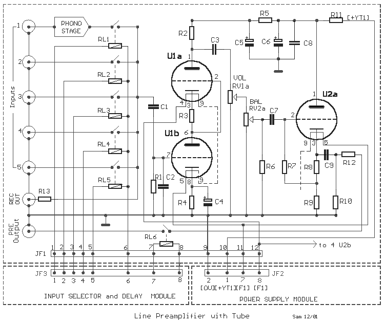
The circuit was designed to create a line preamplifier using double triode tubes. It consists of three parts, including the main preamplifier. The line preamplifier circuit utilizing double triode tubes is structured to enhance audio signals by amplifying low-level signals...
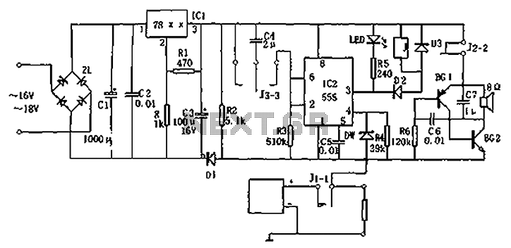
Circuit diagram for a DC power supply protection circuit. The device includes a buck rectifier power supply, a monostable delay circuit, a relay control circuit, and an audio feedback oscillation circuit. The entire circuit operates with a DC voltage...
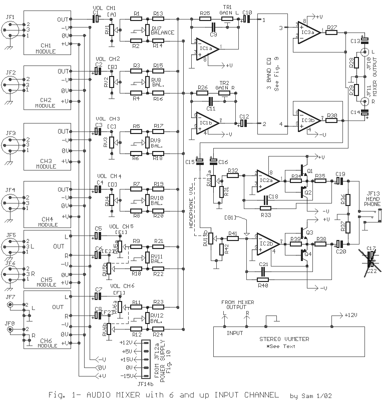
The main circuit of the 6-channel mixer consists of six input channels. Channels 1-4 are mono, while channels 5-6 are designed for music use. The number of input channels can be increased as desired. The output of each channel...
SPI Integrated Circuit Bus, IC Buses, an IC, Chip-to-Chip Bus Serial Peripheral Interface, Integrated Circuit Bus types, and IC Bus Electrical Interface Descriptions. Peripheral Interface (SPI) circuit is a. The Serial Peripheral Interface (SPI) is a synchronous serial communication...
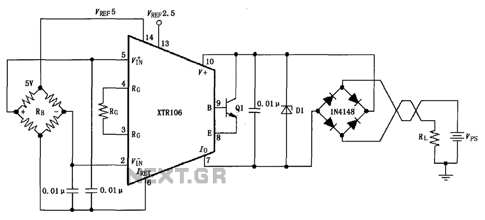
The circuit utilizes a Zener diode D1 to limit surge voltage and incorporates a four-diode rectifier bridge to prevent reverse voltage. The Zener diode D1 is rated at 36V, with optional choices being 1N4753A or 6KE39A. When the loop...
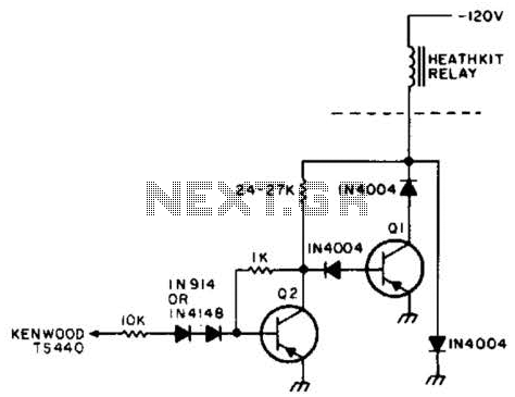
The relay power in the linear circuit is derived from a -120 V bias supply, while the transmit keying output from the Kenwood device is +12 V with a maximum current of 10 mA. A critical component of this...