
3 square waves generator

The schematic for this circuit includes several key components: a crystal oscillator, a series of frequency dividers, an LM555 timer configured in astable mode, a dual timer (556), resistors, capacitors, and JK flip-flops. The crystal oscillator serves as the primary frequency source, providing a stable reference clock. The frequency dividers reduce the clock frequency to the desired level, ensuring that the output frequency is half of the reference clock frequency.
The LM555 timer is configured to operate in astable mode, generating a continuous square wave signal. The duty cycle is adjusted to 50%, which is essential for maintaining equal high and low periods in the output signal. The dual timer (556) is crucial for generating the monostable output pulses. The first timer is set to produce a pulse of duration T/3, while the second timer produces a longer pulse with a duration of 2T/3. The precise timing is achieved through careful selection of resistor and capacitor values according to the formulas provided.
To trigger the timers, a differentiator circuit is employed to create a negative pulse train from the reference clock. This pulse train is then processed through a clipper circuit to ensure that the pulses are of the correct amplitude and shape for reliable triggering of the monostable timers.
The output from the monostable timers is fed into three JK flip-flops, which are configured to toggle their outputs based on the incoming pulse trains. Each flip-flop produces a square wave output that is phase-shifted by 120° relative to the others. This configuration is particularly useful in applications requiring synchronized square wave signals, such as in motor control, phase-locked loops, or signal processing systems. The overall design emphasizes stability, precision, and reliability in generating multiple phase-shifted outputs from a single reference clock source.The circuit provides three square wave outputs with 120° of phase difference between each other. Reference clock frequency is twice that of the required frequency. This can be obtained from a crystal oscillator with a chain of dividers or by using LM 555 in 50% duty cycle astable mode. If 1/T is the frequency of the reference clock, the dual timer 556 is connected to give two mono-stable output pulses of duration T/3 and 2T/3. The first timer R and C value are adjusted so that ta = l.lRaCa = T/3 and the second timer R and C values so that tb = l.lRbCb = 2T/3.
For triggering the two monostables a negative pulse train (1st) is derived from the reference clock with a differentiator and a clipper combination as shown. The three pulse trains trigger three JK flip flops giving three phase square wave outputs.
Related Circuits
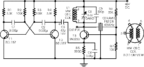
A versatile circuit of an IF signal generator that may be of interest to radio hobbyists and professionals alike. Transistors T1 and T2 form an astable multivibrator oscillating in the audio frequency range of 1 to 2 kHz. An...

Many microcontrollers or PICs have uncommitted digital-to-analog converter (DAC) outputs that can generate sine waves. However, these outputs typically have low resolution (8 to 10 bits), resulting in total harmonic distortion (THD) in the range of 1%. Alternatively, using...
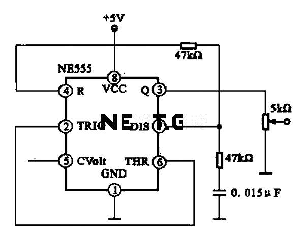
A 1 kHz square wave signal generator is created using a time base circuit with an NE555 timer, combined with a time constant circuit consisting of a 47 kΩ resistor and a 0.15 µF capacitor. The circuit utilizes the...
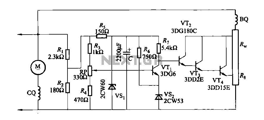
The DC generator automatic voltage regulator circuit is illustrated in Figure 7-53. This circuit is designed for a 40kW, 230V DC shunt complex machine, with a voltage change rate of up to 2.5 percent. In Figure 7-53, BQ represents...
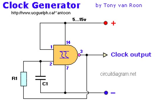
The following diagram is the clock generator circuit diagram built using NAND gate logic integrated circuits (ICs). The circuit can utilize either the IC 7400, which is a TTL type, or the IC 4011, which is a CMOS type....
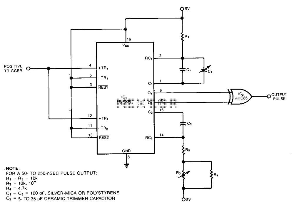
The pulse generator consists of two low-power CMOS chips that produce a precise pulse width ranging from 50 to 500 ns. IC1 is a dual monostable multivibrator (one shot) where each positive trigger pulse initiates simultaneous positive output pulses...