
3 to 12 volts step up DC converter using MAX668
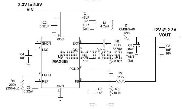
The circuit described is a step-up (boost) DC-DC converter designed to convert an input voltage in the range of 3 to 12 volts into a higher output voltage. The MAX668 integrated circuit serves as the core component for this conversion process, facilitating efficient voltage amplification.
The MAX668 is a high-efficiency boost converter that operates under various load conditions. It typically features a built-in switch, which allows for the regulation and control of the output voltage. The design involves connecting the input voltage source to the input pin of the MAX668, while the output pin is connected to the load requiring the elevated voltage.
Key components of the circuit include the inductor, which stores energy when the switch is closed and releases it when the switch opens, thus boosting the voltage. Capacitors are used for input and output filtering to smooth out voltage fluctuations and improve transient response. Additionally, feedback resistors may be included in the circuit to set the desired output voltage level, ensuring stability and accuracy in voltage regulation.
The circuit operates by switching at a high frequency, typically in the range of hundreds of kilohertz, which allows for the use of smaller passive components and enhances overall efficiency. The MAX668 also includes features such as overvoltage protection and thermal shutdown to safeguard the circuit and connected components.
Design considerations should include selecting appropriate inductor and capacitor values based on the required output current and voltage ripple specifications. Thermal management may also be necessary, depending on the power levels involved and the operating environment.
This step-up converter design is suitable for various applications, including battery-powered devices, portable electronics, and any system requiring a stable higher voltage from a lower voltage source.3 to 12 volts step up DC converter using MAX668 integrated circuit design 🔗 External reference
Related Circuits
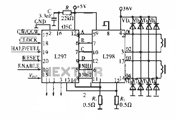
The circuit operates using a dedicated stepping motor controller, the L297. Pin 17 (CW/CCW) is utilized to control the rotation direction of the stepper motor. Pin 18 (CLOCK) regulates the speed of the stepper motor, while pin 19 (HALF/FULL)...
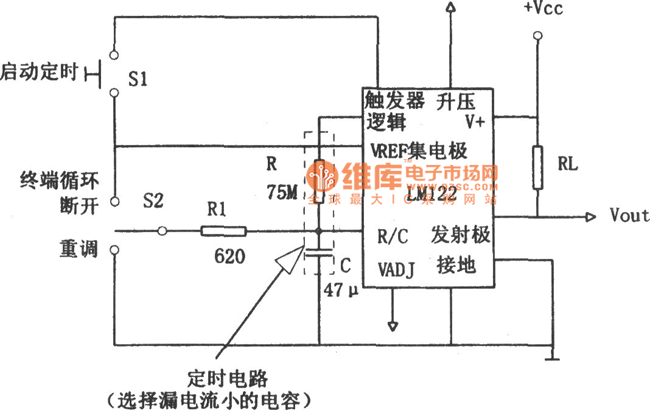
In this figure, S1 initiates the timing process, and once the timer is activated, toggling this switch will not impact the timing operation. S2 serves as the OFF switch located in the center; toggling this switch allows the timer...
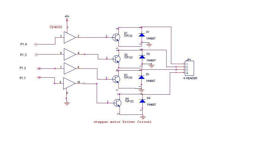
A 6V, 2A stepper motor is utilized in this circuit. The CD4050 hex buffer is employed to connect to the microcontroller. The output of the CD4050 is linked to the base of a TIP122 transistor. The emitter and collector...
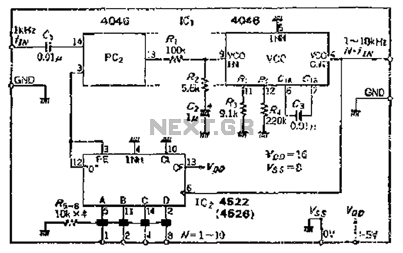
The CMOS IC 4046 Phase-Locked Loop (PLL) operates with a maximum frequency of 1 MHz. It is connected to a programmable divider, allowing it to process input frequencies. As the frequency increases by a factor of t, the circuit's...
The operation of the converter relies on the weighted addition and transfer of the analog input levels to the digital output levels. It comprises comparators and resistors. Although, theoretically, the number of bits is unlimited, each bit requires a...
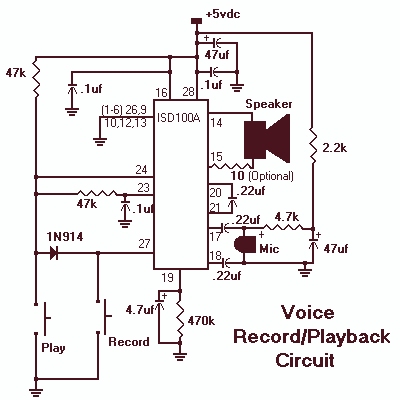
The ISD1000A is a Direct Analog Storage device which allows you to store 20 seconds worth of voice data on an IC chip which can be played back anytime. The data stored will stay in memory even if the...