
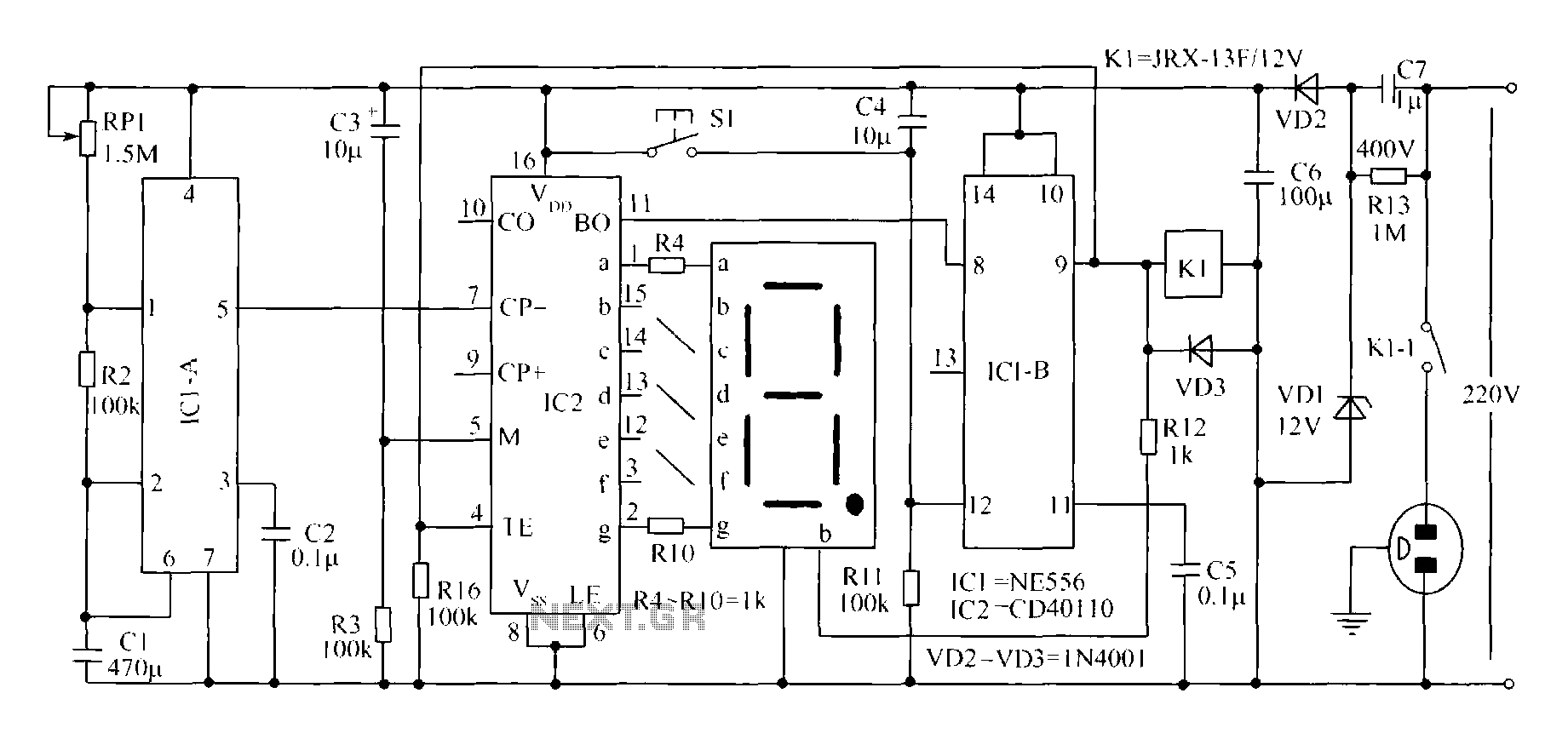
TheCircuit of One-hour Timing Circuit Using LM122
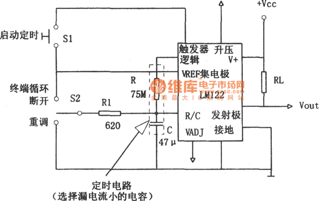
The circuit described incorporates two switches, S1 and S2, which play critical roles in the timer's operation. S1, when engaged, begins the timing sequence, allowing the timer to function without interference. This characteristic is essential for precision timing applications where accidental interruption of the timing sequence must be avoided. The switch S2, positioned centrally, functions as an OFF switch, providing the user with control to halt the timer at any point during its operation.
The timer's operational cycle consists of three distinct phases: charging, open circuit, and discharging. During the charging phase, energy is stored in a capacitor or similar component until a predetermined voltage is reached. The transition to an open circuit indicates that the timer is ready to release its stored energy. In the discharging phase, the stored energy is utilized to perform a specific task, such as activating a relay or powering an output device.
If the charging phase is interrupted—meaning S2 is toggled during this process—the circuit is designed to revert to the operational state of the timer's output. This feature ensures that the timer can resume its function without losing the previous state, thereby enhancing the reliability and efficiency of the circuit in various applications. The careful design of these switches and the timing mechanism is crucial in applications requiring precise control and timing, such as in automated systems, timers, and various electronic devices.In this figure S1 can start timing and when the timer starts, turning this switch has no effect.S2 is the OFF switch in the middle and turning this switch can make the timer complete the procedure: charging-open circuit-discharging. Because of charging stopped halfway, the charging position would return to the work state of the timer s output circuit.
A.. 🔗 External reference
Related Circuits
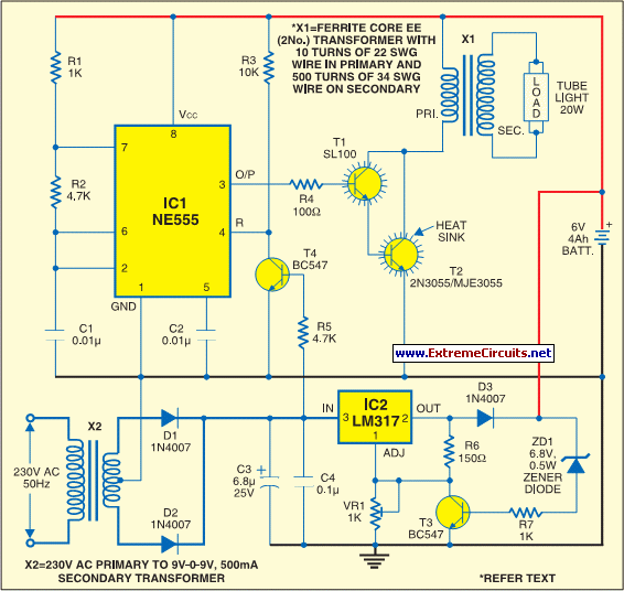
The circuit consists of inverter and charger sections. The inverter section utilizes the NE555 timer, while the charger section is based on the LM317 adjustable regulator. In the inverter section, the NE555 is configured as an astable multivibrator, generating...
An astable multivibrator is an electronic device that continuously alternates between two states in its output. When one state is high, the other is low. This characteristic is useful for generating a continuous stream of pulses without the need...
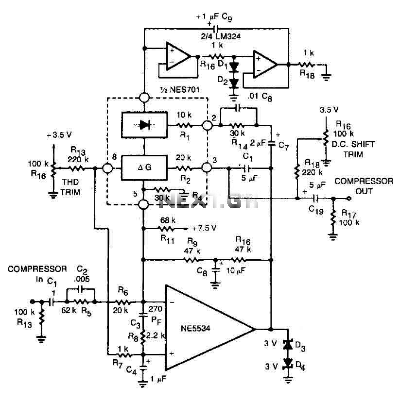
This circuit for a compressor utilizes a high-fidelity external operational amplifier (op amp) with high gain and wide bandwidth. A compensation network at the input is required for stability. The rectifier capacitor (Cg) is not grounded; instead, it is...
A novel timing switch circuit features a "Variable Timing" adjustment function in addition to a standard timing circuit. It also includes a countdown display feature, which indicates the remaining time of the timing circuit, making it particularly useful. The...
This circuit also prevents the shutdown circuit of the IR2161 from operating in the normal way; therefore, an external SCR-based protection circuit needs to be added. The IR2161 is a high-voltage, high-speed driver designed for driving IGBTs and MOSFETs in...
This circuit is a digital voltmeter diagram featuring an LED display. It is designed for measuring the output voltage of a DC power supply. The voltmeter incorporates a 3.5-digit LED display along with a negative voltage indicator. It is...